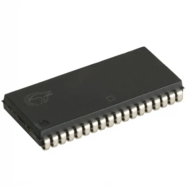
Infineon Technologies CY7C1049GN-10VXI — Memory (DRAM / SRAM / Flash / EEPROM)

Infineon CY7C1049GN-10VXI SRAM, 4 Mbit, 10 ns, 36-SOJ

MPNCY7C1049GN-10VXI
Active

Infineon CY7C1049GN-10VXI, asynchronous SRAM, 4 Mbit (512K x 8), parallel interface, 10 ns access time, 4.5 V to 5.5 V supply, -40°C to 85°C, 36-SOJ (BSOJ) package, Tube.

$7.0800Ref. price · indicative, final on quote
Packaging36-BSOJ (0.400", 10.16mm Width)
RoHSROHS3 Compliant
Independent supplier — new & surplus stockAuthenticity-screened · ESD-safe packingListing updated Aug 2026

Specifications

CY7C1049GN-10VXI specifications
ParameterValue
Memory typeVolatile
MountingSurface Mount
Supply voltage4.5V ~ 5.5V
Memory interfaceParallel
Operating temperature-40°C ~ 85°C (TA)
PackageTube
TechnologySRAM - Asynchronous
Access time10 ns
Memory size4Mbit
Memory formatSRAM
Case36-BSOJ (0.400\", 10.16mm Width)
Memory organization512K x 8
Write cycle time - word, page10ns

Product details

For a system architect, that margin allows the memory to sit on a shared bus with a 50 MHz to 66 MHz controller without wait states, assuming reasonable board trace lengths.

36-SOJ package — rework and layout notes

The 36-SOJ (Small Outline J-lead) package, 0.400-inch body width, is a through-hole-friendly surface-mount form factor. The J-leads are visible and accessible to a hot-air station, making hand rework straightforward — no hidden balls, no underfill. The 10.16 mm width fits standard SOJ footprints; verify the pad pitch against your existing layout if replacing a 32-pin or 44-pin SOJ part. The package ships in Tube, so plan for pick-and-place feeder changeover if your line runs tape-and-reel exclusively.

Temperature grade and supply — where it works

At 5 V the 10 ns timing is specified; dropping to 4.5 V may add a small derating, though the datasheet holds the same 10 ns across the full range.

For dual-sourcing resilience, the CY7C1049G-10VXI is a functional equivalent — same 4 Mbit density, 10 ns speed, 5 V supply, and 36-SOJ package — differing only in the lead-free finish code (the 'GN' suffix indicates NiPdAu plating).

Frequently asked questions

What is the access time of CY7C1049GN-10VXI?

The access time is 10 ns for both read and write cycles (word and page write), allowing zero-wait-state operation with bus controllers up to about 66 MHz.

What is the equivalent or replacement for CY7C1049GN-10VXI?

The 'GN' suffix on this part indicates NiPdAu lead finish; the 'G' variant uses a different plating. Both are active and cross-compatible for the same socket.