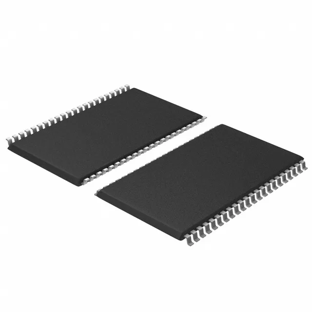
What this 5 V asynchronous SRAM brings to the board
The parallel interface and 44-TSOP II footprint are a known quantity on legacy telecom line cards, industrial controller boards, and test equipment where the memory bus hasn't migrated to 3.3 V or DDR.
10 ns access — timing closure and bus margin
For a 50 MHz bus with a 20 ns cycle, the part has 10 ns of address-to-data valid time, which leaves about 4 ns to 5 ns of margin after accounting for PCB trace delay and clock skew. At 66 MHz (15 ns cycle), that margin shrinks to 2 ns or less — the layout engineer needs to keep the address and control traces short and matched.
Industrial temperature and the 5 V rail
The 5 V I/O also makes it a drop-in for legacy 5 V logic buses without external translation.
Package and footprint — 44-TSOP II
The 44-TSOP II package (0.400-inch body width, 10.16 mm) is a standard asynchronous SRAM footprint shared across many 4 Mbit and 8 Mbit parts from Cypress, ISSI, and Alliance Memory. The 16-bit data bus and 18 address lines come out in a familiar pinout that a layout engineer can route with two signal layers on a typical four-layer board.
For a BOM that needs a 5 V asynchronous SRAM in the 44-TSOP II footprint, this part is a straightforward line-item that can be sourced through independent distribution without obsolescence risk.