It means the SRAM can deliver data within 10 ns of the address being valid, which is fast enough to feed a 100 MHz bus without wait states in most cache or FIFO applications. If your processor or FPGA runs a memory controller at 66 MHz or below, this part gives you a full cycle of timing margin on the data setup.
256K x 16 organization — matches a 16-bit bus directly
The 4 Mbit memory is organized as 256K words of 16 bits each. That x16 data bus width connects straight to a 16-bit microcontroller or DSP without needing byte-lane muxing. For a 32-bit bus, two of these parts side by side give you a 32-bit wide memory array with a shared address bus.
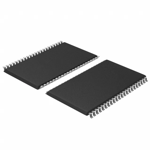
44-TSOP II — footprint and handling
The 44-TSOP II package (0.400-inch body width, 10.16 mm) is a standard JEDEC footprint for asynchronous SRAMs. It is surface-mount, so it reflows with the rest of the board.