4 Mbit async SRAM for the 1.8 V bus
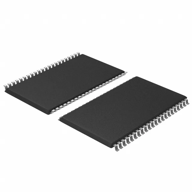
It runs on a 1.65 V to 2.2 V supply, which puts it on the 1.8 V nominal rail — common in low-power DSPs, FPGAs, and application processors that need fast scratchpad or packet buffer memory without the overhead of a synchronous clock. The 44-pin TSOP II package (0.400-inch body, 10.16 mm height) is a standard footprint for this density class; it reflows with a standard profile and is hand-solderable with a fine tip if you are careful.
15 ns access — timing margin for a 50–66 MHz bus
On a 50 MHz bus (20 ns cycle), that leaves about 5 ns of margin after accounting for address-to-chip-enable and output-enable delays — tight but workable if the PCB trace lengths are kept under 3 inches and the load capacitance is reasonable. At 66 MHz (15 ns cycle), you are cycle-bound; the part still works if the controller inserts one wait state.
Industrial temperature, active lifecycle
If you are dual-sourcing, the base part number CY7C1041 covers the family; the G18 suffix indicates the 1.8 V supply variant and the -15ZSXI speed/package/temperature code.