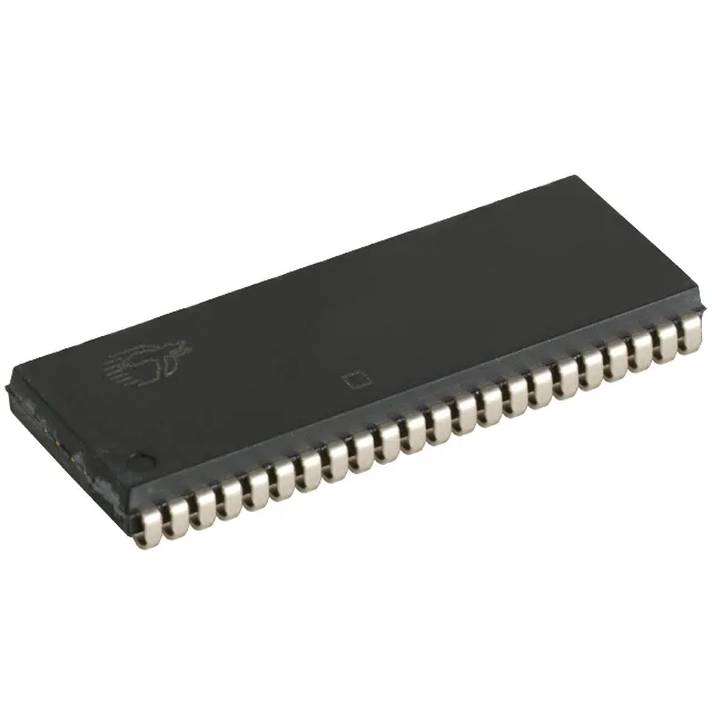
The Infineon CY7C1041G18-15VXIT is a 4Mbit asynchronous SRAM organized as 256K x 16, with a 15 ns access time that sets the pace for the memory bus. That 15 ns window means the host controller can grab data inside a single fast clock cycle — think 66 MHz or slower — without inserting wait states. For a 1.8V-core CPU or FPGA that needs scratchpad or look-up table memory, this part matches the timing budget cleanly. It is a volatile memory, so contents vanish on power loss; plan for a backup battery or non-volatile store if the data must survive a reset.
Supply voltage: 1.65V to 2.2V — not a 3.3V part
This SRAM runs on a 1.65V to 2.2V supply rail, which puts it squarely in the 1.8V-logic domain. It is not compatible with 3.3V I/O without a level shifter — the absolute maximum on the pins is the supply rail plus a diode drop, so plugging it into a 3.3V bus will let the magic smoke out. If your design uses a 1.8V-core FPGA or a low-voltage SoC, this part is a natural fit. The narrow supply range also means the decoupling needs to be tight: a 0.1 µF ceramic right at each VDD pin, plus a bulk cap nearby.
The 85°C ceiling is the upper limit for the ambient air around the part — junction temperature will be a few degrees higher, but within the die rating. No need for a fan or heatsink at normal airflow; just keep the board layout clean and avoid hot spots from adjacent power devices.
Package: 44-SOJ — verify the footprint
The package is a 44-lead SOJ (Small Outline J-lead) in a 0.400-inch body width. That is not the common 0.300-inch SOIC footprint — the J-leads curl under the body, so the land pattern is different. If you are replacing a TSOP or BGA SRAM, the board layout will need a respin. Surface-mount only; no socket option unless you find a custom SOJ socket.
Lifecycle: active — no LTB worry
No last-time-buy clock is ticking, and no end-of-life notice has been issued. The base product number is CY7C1041, which covers the full family of density and speed variants.