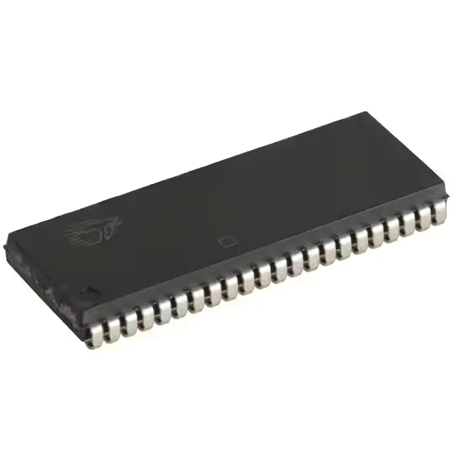
Infineon Technologies CY7C1041CV33-15VXC — Memory (DRAM / SRAM / Flash / EEPROM)

Infineon CY7C1041CV33-15VXC 4Mbit Async SRAM, 15 ns, 44-SOJ

MPNCY7C1041CV33-15VXC
Active

Infineon CY7C1041CV33-15VXC, 4Mbit asynchronous SRAM, 256K x 16 organization, 15 ns access time, parallel interface, 3V to 3.6V supply, 44-BSOJ (0.400") surface-mount package, 0°C to 70°C commercial temperature range.

$4.6715Ref. price · indicative, final on quote
Independent supplier — new & surplus stockAuthenticity-screened · ESD-safe packingListing updated Aug 2026

Specifications

CY7C1041CV33-15VXC specifications
ParameterValue
Memory typeVolatile
MountingSurface Mount
Supply voltage3V ~ 3.6V
Memory interfaceParallel
Operating temperature0°C~70°C(TA)
PackageTube
TechnologySRAM - Asynchronous
Access time15 ns
Memory size4Mbit
Memory formatSRAM
Case44-BSOJ (0.400\", 10.16mm Width)
Memory organization256K x 16
Write cycle time - word, page15ns

Product details

15 ns access time — timing margin for zero-wait-state operation

For a 50 MHz bus with a 20 ns cycle, the 15 ns access leaves a 5 ns margin for PCB trace delay and clock skew — enough for a clean layout on a two-layer board but tight if long traces or multiple loads are on the bus.

256K x 16 organization — address and data bus width

With a 256K x 16 organization, this part presents an 18-bit address bus and a 16-bit data bus. That 16-bit width matches processors with a 16-bit external data bus directly; for 8-bit or 32-bit controllers, two devices can be paired for 32-bit width or byte-lane control is handled by the upper address bits. The 4 Mbit density provides 512 KB of storage, enough for boot code shadowing, packet buffers, or display frame storage in mid-complexity embedded systems.

No level translation is needed on the address or data lines when interfacing to a 3.3 V FPGA, ASIC, or MCU memory controller.

44-SOJ package — footprint and assembly

The 44-SOJ package uses J-leads on a 0.400-inch (10.16 mm) wide body, with a standard 1.27 mm pitch. It is a surface-mount package that reflows with conventional solder profiles. The SOJ footprint is well-established in memory modules and embedded boards; the J-lead form factor provides good coplanarity and visual solder-joint inspection.

Frequently asked questions

What is the access time of CY7C1041CV33-15VXC?

The access time is 15 ns, and the write cycle time for word and page operations is also 15 ns. This speed grade supports zero-wait-state operation with processor buses up to approximately 66 MHz, assuming reasonable PCB trace lengths.

Can CY7C1041CV33-15VXC operate at 3.3V?

The device is designed for 3.3 V logic systems and does not require level shifters on the memory interface.

What is the exact replacement for CY7C1041CV33-15VXC?

Since the part is Active, the current order code remains the recommended procurement target. For a pin-compatible alternative within the same family, consult the base product number CY7C1041 for other speed or temperature variants.