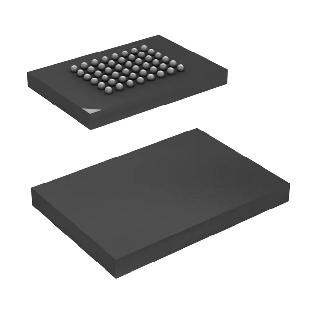
10 ns asynchronous SRAM for high-throughput cache and buffer applications
This part is a drop-in for any 3.3 V parallel SRAM socket needing fast random access — think network processor look-aside buffers, FPGA block-RAM expansion, or DSP scratchpad memory where deterministic latency matters more than sequential throughput. The 10 ns cycle time means the memory can keep pace with a 100 MHz bus without wait states, provided the controller's output hold time and setup budget are met.
48-TFBGA footprint and rework considerations
The 48-TFBGA package (7x8.5 mm body, 0.5 mm ball pitch) demands careful PCB layout and rework discipline. For the PCB layout engineer: route the 16-bit data bus and address lines with matched trace lengths to avoid skew on the 10 ns window; place decoupling capacitors within 2 mm of the BGA ball field — a 0.1 µF ceramic per supply pin pair, plus a 4.7 µF bulk cap near the package edge. Hot-air rework stations need a bottom-side preheat to 100°C to prevent cold joints on the inner balls.
For the procurement buyer, this removes the single-source risk flag that obsolete SRAMs carry — you can qualify this part into a new BOM without planning a future respin. The base product number CY7C1041 covers a family of density and speed variants; if your design later needs a different speed grade or package, the family shares the same die and interface, simplifying second-source qualification within the series.
For a system architect clocking a 100 MHz bus (10 ns period), this leaves zero margin for address decoding, PCB trace delay, and input setup at the controller — so a 10 ns SRAM is realistically a fit for buses running at 66 MHz or slower unless the controller has a programmable wait-state generator. The 256K x 16 organization gives a 16-bit word width, which halves the pin count versus a byte-wide part for the same density — useful when the FPGA or ASIC has limited I/O banks. The parallel interface is straightforward: no clock, no command sequences — just chip enable, output enable, write enable, and the address/data bus. This simplicity is the reason asynchronous SRAM still appears in latency-critical paths where SDRAM's refresh overhead is unacceptable.