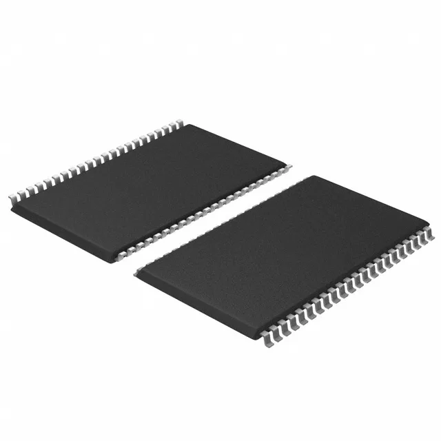
The CY7C1021CV33-15ZXC: Packaged in a 44-TSOP II (10.16 mm width) surface-mount footprint, this part was used for buffer memory, cache tag storage, and general-purpose data buffering in embedded systems, telecom line cards, and industrial controllers that needed fast, simple, byte-wide or word-wide memory without refresh overhead.
For a system running a 33 MHz or 40 MHz bus clock (30 ns or 25 ns period), this leaves 10 ns to 15 ns of setup margin before the next clock edge — comfortable for most glue-logic interfaces. If your legacy design was originally specified for a 12 ns or 10 ns part, this 15 ns variant may not meet timing closure; verify the address-to-clock setup window in your worst-case temperature and voltage corner.
If you are qualifying this for a new design, look for a pin-compatible 1 Mbit asynchronous SRAM in 44-TSOP II from a current-production family (e.g., the Alliance Memory or ISSI equivalents that share the same footprint and 3.3 V supply).
Package and footprint — the mechanical constraint
Any replacement must match this footprint — pin 1 location, pitch, and body dimensions — to avoid a board respin. The shipping medium is listed as Bag, which is typical for tray or tube quantities; this does not affect the device package itself.