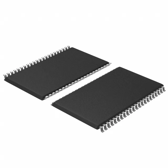
What this 1Mbit SRAM does in a 3.3V bus
The CY7C1021BV33-12ZC is a 1Mbit asynchronous SRAM organized as 64K x 16 bits, with a 12 ns access time that sets the minimum read-cycle window for the host controller. The 16-bit-wide data bus eliminates the need for byte-lane muxing on 16-bit MCUs or DSPs, saving two glue-logic packages per board. Supply range is 3.0V to 3.6V, making it a direct fit in a 3.3V memory bus without level translation. The 12 ns write cycle time matches the read access, so back-to-back read-write sequences run at the same cycle budget — no asymmetrical timing penalty. This matters for real-time control loops where the processor alternates between fetching code and logging data.
Commercial temp grade — indoor deployment only
No margin for extended industrial or automotive environments; if the board sees an engine bay, outdoor enclosure, or unheated warehouse, this package will not hold its timing specs at the cold or hot end. The 44-TSOP II package (0.400-inch body width, 10.16 mm) is a thin small-outline profile common on 1990s–2000s SRAM designs. It is surface-mount but not a fine-pitch BGA — rework with standard hot-air tools is straightforward, though the pin pitch still needs a soldermask-defined pad and careful stencil alignment.
Infineon lists this part as Obsolete. The only sourcing channel is independent distribution or excess inventory held by brokers. Because the part is obsolete, verify date code and traceability before committing to a production run. Moisture sensitivity level for TSOP II is typically MSL-3; if the parts have been stored for more than two years, a bake per J-STD-033 may be needed before reflow.