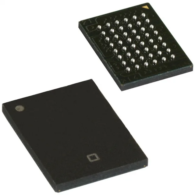
12 ns async SRAM for industrial cache and scratchpad
The 16-bit-wide word organization matches 16-bit MCU and FPGA buses directly, eliminating the need for external byte-lane multiplexing and simplifying the memory interface.
In a system with a 50 MHz bus clock (20 ns period), a 12 ns access leaves 8 ns of timing margin for address propagation, signal settling, and setup/hold before the next clock edge. That margin shrinks if the board has long trace runs or multiple loads on the data bus — the 12 ns rating gives the layout engineer a realistic budget for fanout and decoupling.