Memory density and bus organization for the BOM
The CY62147DV30LL-45BVXI: The 4-Mbit density organized as 256K x 16 bits means the part presents a 16-bit-wide data bus to the controller — a natural fit for 16-bit microcontrollers or as a word-wide scratchpad alongside a 32-bit processor where you want to minimise the chip count per memory bank. The parallel interface requires 18 address lines plus 16 data lines; the 45 ns access time and 45 ns write cycle set the bus timing budget for the memory controller's setup-and-hold window.
Supply voltage and temperature grade — what they mean for fit
Because the part is asynchronous, there is no clock tree to tune — the read and write cycles are strobe-controlled by the chip-enable and write-enable signals. This simplifies the PCB timing closure compared to a synchronous SRAM of the same density, especially when the host controller has no dedicated SDRAM controller on-chip.
Package footprint and board integration
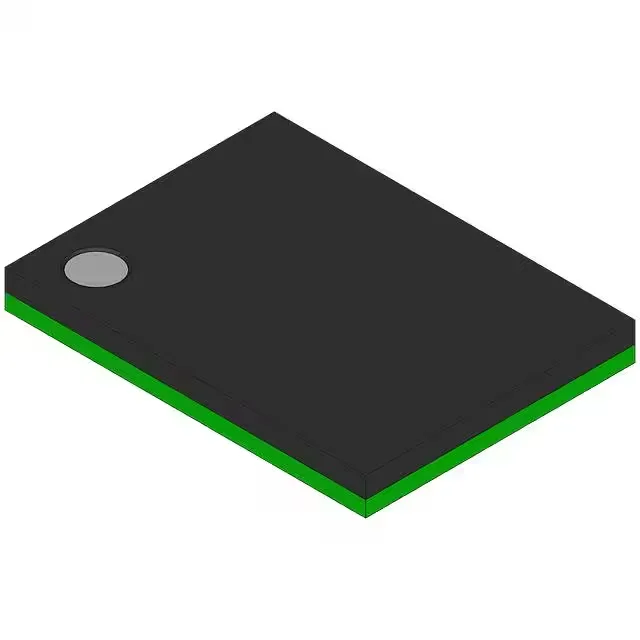
The 48-ball VFBGA with a 6 mm x 8 mm body and 0.75 mm ball pitch is a fine-pitch BGA that routes out on two signal layers with a single via per ball if the escape pattern is optimised.
Active production and compliance posture
ROHS3 compliant means the plating and mould compound are free of the ten restricted substances including the four phthalates added in the 2015 EU amendment; no exemption declarations are needed for EU-market equipment. As an active MoBL® series member, the CY62147DV30LL-45BVXI is supported for new designs and ongoing production.