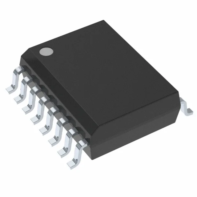
The Cypress CY14B101Q3-SFXI is a 1 Mbit non-volatile SRAM (NVSRAM) organized as 128K x 8 bits, accessed through an SPI interface running at 40 MHz. It combines the fast read/write cycle of a standard SRAM with non-volatile storage, so data is retained after power loss without a battery. Typical applications include configuration storage, parameter logging, and data buffering in industrial controllers, metering, and telecom equipment where the combination of fast write speed and non-volatility eliminates the need for EEPROM or battery-backed SRAM.
SPI at 40 MHz — throughput and bus margin
The 40 MHz SPI clock rate gives a raw serial throughput of 40 Mbit/s. For a 128 KB read or write, that translates to roughly 26 ms transfer time before the internal non-volatile store cycle. The SPI interface uses the standard four-wire protocol (SCK, SI, SO, CS), so it connects directly to any MCU or SoC with an SPI master. No special timing tweaks are needed at 40 MHz with a 3.3 V supply, but keep the trace length under 10 cm and add a series resistor near the source to damp reflections if the bus also drives a second SPI slave.
NVSRAM vs FRAM — a genuine cross-shop decision
The closest functional peer is the FM25VN10-G, a 1 Mbit serial FRAM from Cypress (now Infineon). Both parts are 1 Mbit non-volatile memories with an SPI interface at 40 MHz and the same 128K x 8 organization. The key difference is the storage technology: NVSRAM uses a SONOS transistor cell, while FRAM uses a ferroelectric capacitor. In practice, the NVSRAM offers essentially unlimited write endurance (the datasheet typically specifies 1e12 cycles), while FRAM endurance is also very high (1e14 cycles). The NVSRAM has a slightly higher supply voltage floor at 2.7 V versus 2.0 V for the FRAM.
SOIC-16 package — board footprint and assembly
The part comes in a 16-pin SOIC package, surface-mount only. The SOIC-16 footprint is standard and widely supported in assembly houses. No exposed pad or thermal slug — the package dissipates through the leads, so no special via stitching is needed.