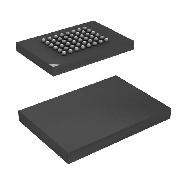
It combines the fast read/write cycle of an SRAM with non-volatile storage, eliminating the need for a backup battery in designs that must retain data through power loss.
45 ns cycle — timing margin in a parallel bus
The 45 ns access time and 45 ns write cycle time (word/page) set the bus timing budget. For a system running a 20 MHz to 25 MHz bus, this gives roughly one clock cycle of margin after accounting for PCB trace delay and output hold times. If the design uses a faster memory controller (e.g., 50 MHz), the 45 ns part may force a wait state insertion — verify against the controller's setup/hold requirements. The parallel interface is straightforward to connect to most 8-bit MCUs and FPGAs, with no serial protocol overhead.
For BOM planning, this part can be qualified into new designs without an immediate obsolescence watch. The NVSRAM format is a proprietary Cypress technology, so if a second-source is needed, the closest functional alternative is a battery-backed SRAM or a serial FRAM — but neither is a drop-in replacement for the parallel NVSRAM footprint.
Package and footprint — 48-ball FBGA
The 0.8 mm ball pitch is common for memory BGAs; the footprint matches Cypress's standard 48-FBGA layout for this density. Decoupling with a 0.1 µF ceramic per supply pin, placed as close to the balls as the via pattern allows, keeps switching noise within spec.