Noise figure and gain — the selection anchors
The BFP843FH6327XTSA1: Noise figure spans 0.8 dB to 1.7 dB across 450 MHz to 10 GHz. At 450 MHz the 0.8 dB floor means the transistor adds negligible noise to a GPS or cellular LNA input stage; at 10 GHz the 1.7 dB figure still keeps the cascaded NF below 2 dB in a well-matched design. Gain ranges from 13.5 dB to 25 dB over the same frequency band. The 25 dB peak at the low end suits a single-stage LNA for ISM-band or cellular low-band; the 13.5 dB at 10 GHz means a two-stage chain is needed to reach typical system gain targets in Ku-band downconverters. Collector-emitter breakdown is 2.25 V maximum. This sets the supply rail ceiling at 1.8 V to 2.0 V for linear operation — the transistor is a low-voltage SiGe device, not a general-purpose RF part. The 55 mA maximum collector current supports bias points up to 30-40 mA for moderate linearity in a common-emitter LNA. DC current gain (hFE) is 150 minimum at 15 mA, 1.8 V. This guarantees a beta floor for bias network design — a base current of 100 µA at the 15 mA bias point is predictable across temperature and process corners.
Package and thermal budget for the BOM
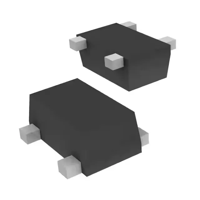
Housed in the PG-TSFP-4-1 package, a 4-lead flat-lead SMD with a small footprint suited for dense RF layouts. The 150 °C junction temperature rating provides headroom: at 125 mW maximum power dissipation and a typical RthJA around 300 K/W, the junction rise stays under 40 °C above ambient, keeping the die below 110 °C in a 70 °C enclosure. Surface-mount assembly with standard reflow profiles — the flat-lead package requires no special stencil aperture beyond the manufacturer's footprint recommendation.