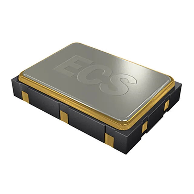
5 MHz HCMOS clock source — enable/disable control included
The ECS-2520S25-050-FN-TR: At 7 mA maximum supply current, it draws enough to drive one or two standard TTL/CMOS clock inputs directly — the HCMOS output stage eliminates the need for external termination on most bus architectures.
The 4-SMD no-lead package sits 1.00 mm above the board when reflowed — the seated height constrains routing beneath the part to passive components under 0.80 mm or clearance traces only. Solder joint reliability is governed by the board-level thermal profile rather than any datasheet limit on the part itself — the 1.00 mm height gives some compliance margin for boards that see thermal cycling.
HCMOS output — drive budget and disable current
HCMOS output drives into standard CMOS/TTL loads without external pull-ups or terminators at frequencies below 20 MHz — the 5 MHz output sits well within the safe toggle rate. The 10 µA maximum supply current in disable mode means standby leakage is negligible compared to the rest of the digital rail, so gating the oscillator on and off saves real current on battery-powered nodes that only need the clock intermittently. Draw 7 mA when enabled and 10 µA when disabled — that 700:1 ratio is the design win for power-cycled sensor nodes and remote telemetry units.