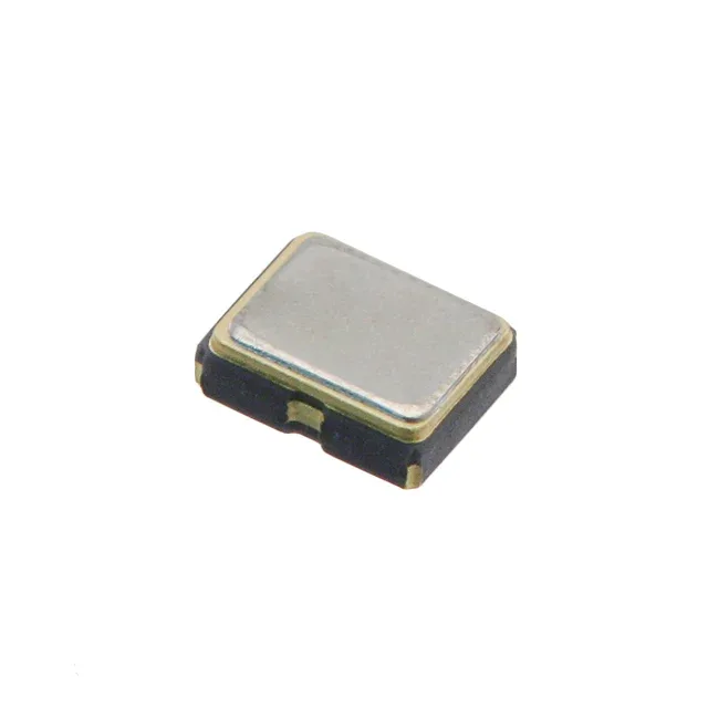
ECS Inc. ECS-2033-120-BN — Crystals & Oscillators

ECS-2033-120-BN 12 MHz CMOS Oscillator, 3.3 V

MPNECS-2033-120-BN
Active

ECS Inc. ECS-2033 XO oscillator, 12 MHz, CMOS output, 3.3 V supply, ±50 ppm, 4-SMD 2.50 x 2.00 x 0.90 mm, Enable/Disable function, Active.

$2.9600Ref. price · indicative, final on quote
Independent supplier — new & surplus stockAuthenticity-screened · ESD-safe packingListing updated Aug 2026

Specifications

ECS-2033-120-BN specifications
ParameterValue
TypeXO (Standard)
SeriesECS-2033
MountingSurface Mount
Supply voltage3.3V
Current - supply7mA
Current - supply (Disable)10µA
Frequency12 MHz
Frequency stability±50ppm
Operating temperature-40°C~85°C
Size (Dimension)0.098\" L x 0.079\" W (2.50mm x 2.00mm)
Height - seated0.035\" (0.90mm)
OutputCMOS
PackageTape & Reel (TR); Cut Tape (CT)
FunctionEnable/Disable
Base resonatorCrystal
Case4-SMD, No Lead

Product details

±50 ppm stability and what it costs in timing budget

The ECS-2033-120-BN: For a UART clocking a 115200 baud link, that drift sits comfortably inside the ±2 % baud-rate tolerance most UARTs spec. For a USB PHY reference, the tolerance is tighter than USB Full-Speed allows on its own — the oscillator would need a PLL or spread-spectrum clock to meet USB spec, since USB requires ±500 ppm at the host.

Current draw — active and disabled

Maximum supply current is 7 mA when the oscillator is running, and drops to 10 µA when disabled — so shutting down the reference eliminates essentially all the quiescent draw. For a battery-powered node that wakes periodically and needs a clean clock during activity, the enable/disable pin is the primary power-control lever; the 10 µA disabled current is low enough to leave the oscillator permanently in the disabled state between wake cycles rather than removing the supply rail entirely.

2.50 × 2.00 mm ultra-thin package

The 4-SMD no-lead package seats at 0.90 mm max height — the thin profile suits portable or handheld hardware where vertical clearance is constrained. No-lead construction means the GND pads sit flush to the board, which helps thermal dissipation to the pad plane but requires a reflow profile with a flat soak to avoid tombstoning on the small pad geometry. Tape-and-reel and cut-tape packaging options are both listed, so the part handles both high-volume SMT assembly and low-quantity prototype reel.

Frequently asked questions

What does the Enable/Disable function actually do in a circuit?

The enable pin gates the output without removing the 3.3 V supply. When disabled the output goes high-Z and current drops to 10 µA max; when re-enabled the oscillator starts and settles within the specified stability band. This is the standard power-control pattern for clocking domains that need to be dropped in sleep modes without a full rail toggle.

Can I use the 12 MHz CMOS output directly as a USB Full-Speed reference clock?

No — the ±50 ppm frequency stability of this oscillator does not meet USB Full-Speed timing requirements, which demand ±500 ppm at the device level. A USB crystal or TCXO with tighter stability is required for USB Full-Speed operation without PLL compensation.