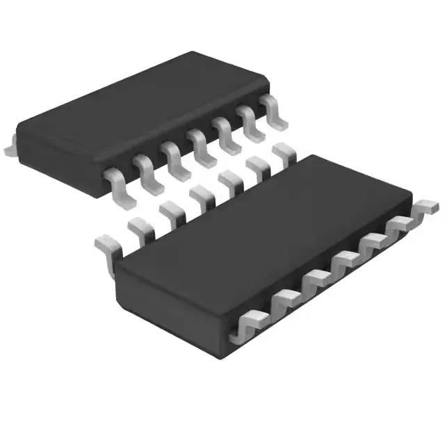
Quad op-amp for multi-channel signal conditioning
The LT1885CS#PBF is a quad general-purpose operational amplifier from Analog Devices' LT® series, packing four independent amplifiers into a single 14-SOIC package. With a 2.2 MHz gain-bandwidth product and a 1 V/µs slew rate, it handles audio-band filtering, sensor buffering, and multi-channel data-acquisition front-ends where each channel needs its own amplifier. Each of the four amplifiers draws 850 µA of supply current, keeping the total quiescent draw under 3.4 mA for the package — a reasonable budget for a 14-pin SOIC on a mixed-signal board where thermal rise from the op-amp section stays low.
DC precision and output swing that matter for the BOM
Input offset voltage is trimmed to 30 µV typical, and input bias current is 150 pA typical — the offset error is low enough that a gain-of-100 stage adds only 3 mV of DC error at the output, and the bias current won't shift the operating point of a 10 kΩ source by more than 1.5 µV. The rail-to-rail output stage swings within millivolts of both supply rails, preserving headroom in low-voltage designs. Output current is rated 50 mA per channel, enough to drive a 600 Ω load or the input of a successive ADC without an extra buffer. Supply range spans 2.7 V to 36 V single supply, or ±1.35 V to ±18 V split supply — the same part works in a 3.3 V battery-powered logger or a ±15 V industrial control board, simplifying BOM consolidation across voltage domains.
Package, temperature grade, and compliance
Housed in a 14-lead SOIC (0.154″ width, 3.90 mm body) with supplier device package designation 14-SO, the LT1885CS#PBF is a surface-mount part shipped in tube format. The 0°C to 70°C commercial temperature range suits controlled indoor environments — benchtop instrumentation, lab equipment, or telecom line cards in climate-controlled shelters.