Active production — BOM-fit note
The V40PW22C-M3/I is an active Vishay dual common-cathode Schottky rectifier rated 20 A per diode at 200 V reverse, with a forward drop of 970 mV at full current. The AEC-Q101 qualification means it is screened for the -40 to 175 °C junction range and automotive reliability stress — suitable for under-hood DC-DC converters, alternator rectification, and reverse-battery protection where the thermal cycle profile matches the automotive discrete standard.
Forward drop and thermal budget
At 20 A per diode the 970 mV forward drop produces about 19.4 W of conduction loss per die. The SlimDPAK (TO-252 derivative) relies on the cathode tab soldered to the PCB copper area to sink that heat. The 175 °C junction rating gives headroom, but the real junction temperature depends on the board's thermal pad size and the ambient under the hood — a 1 oz copper pad with minimal thermal vias will push the die close to the limit at full load.
Reverse leakage at temperature
The 250 µA reverse leakage at 200 V is specified at 25 °C. Schottky leakage doubles roughly every 10 °C, so at 125 °C junction the leakage can exceed 10 mA — enough to add measurable standby loss in a system that idles hot. The trade-off against a fast-recovery silicon diode is lower forward drop at low current but higher leakage at elevated temperature.
Package and PCB layout
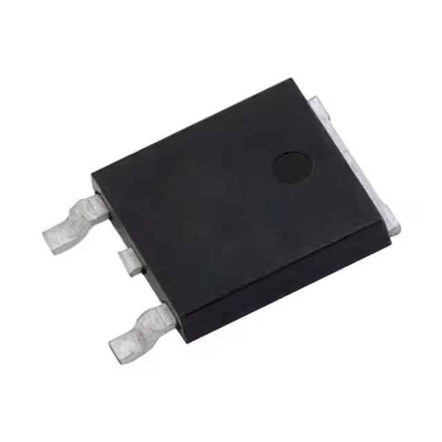
The TO-252-3 (DPak) footprint with the SlimDPAK variant has the cathode tab as the common terminal for both diodes. The two anode pads are separate — the layout must keep the high-current anode traces isolated and the tab connected to the output rail with a wide copper pour.