80V, 430A N-Channel TrenchFET — conduction loss and switching profile
The SQJQ184ER-T1_GE3: The max Rds(on) is 1.4 mOhm at 20 A, 10 V gate drive — this conduction loss figure is the primary spec for a high-current load switch or OR-ing diode replacement, where the voltage drop at full load directly sets the thermal budget. Gate charge totals 240 nC at 10 V, with input capacitance of 16009 pF at 25 V drain bias. The high gate charge means the driver must supply peak current to charge the gate quickly — for a 100 kHz switching frequency the average gate drive current is 24 mA, within the capability of many automotive gate drivers, but the peak current at turn-on may require a gate resistor to manage ringing. The 600 W power dissipation at the case (Tc) sets the upper thermal limit; the actual safe operating area depends on heatsinking and ambient temperature.
AEC-Q101 qualification and temperature range
The 175°C Tj max allows operation in engine bays without derating the current below the 430 A headline, provided the case temperature stays within the thermal impedance limits of the PowerPAK 8x8 package.
PowerPAK 8x8 — package and board integration
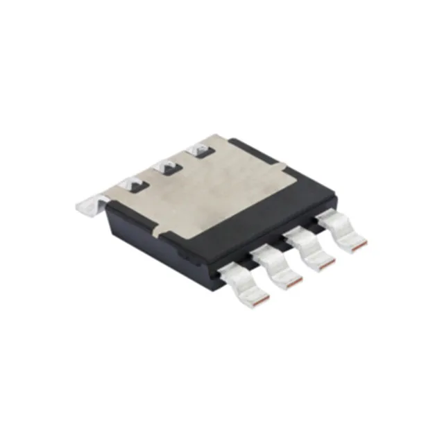
The 8-PowerSMD gull-wing package (PowerPAK 8x8) with a large exposed drain pad on the bottom requires a copper land pattern that matches the pad dimensions for thermal conduction — the datasheet's recommended footprint includes a solder-paste stencil aperture that covers 70-80% of the pad area.
Active lifecycle — sourcing posture
As a single-source Vishay TrenchFET, no direct pin-compatible second-source is listed, but the SQJQ160E-T1_GE3 (60 V, 0.85 mOhm) is a functional peer for lower-voltage designs — the 80 V rating of this part provides margin for 48 V or 72 V battery systems.