20 V N-channel TrenchFET — the switching-loss sweet spot
The SQA446CEJW-T1_GE3: It targets low-voltage power switching where Rds(on) and gate charge both matter — the 17.5 mOhm max on-resistance at 4.5 V gate drive keeps conduction loss under 1.6 W at full current, while the 10 nC typical gate charge at 4.5 V means the driver doesn't waste a switching cycle charging the gate. The AEC-Q101 qualification covers the -55 °C to 175 °C junction temperature range — this is the under-hood automotive band. An engine-bay ECU or transmission controller that sees 125 °C ambient still has 50 °C of margin before derating kicks in.
Rds(on), gate charge, and the drive voltage window
Rds(on) is specified at two drive voltages: 17.5 mOhm max at 4.5 Vgs, 4.5 A Id. The drive voltage window of 2.5 V (minimum for rated Rds(on)) to 4.5 V (maximum) means a 3.3 V logic-level gate drive will barely turn it on — the 2.5 V threshold is 1.3 V max at 250 µA, so a 3.3 V rail gives about 2 V of overdrive, enough to hit the 4.5 V Rds(on) curve only if the driver can source the 10 nC gate charge fast enough. Input capacitance is 910 pF typical at 10 V Vds — that's the load the gate driver sees during switching. Combined with the 10 nC gate charge, the switching energy per cycle is low enough that 500 kHz+ operation is feasible without a heatsink, provided the PCB copper area under the PowerPAK SC-70W-6 dissipates the 13.6 W max power.
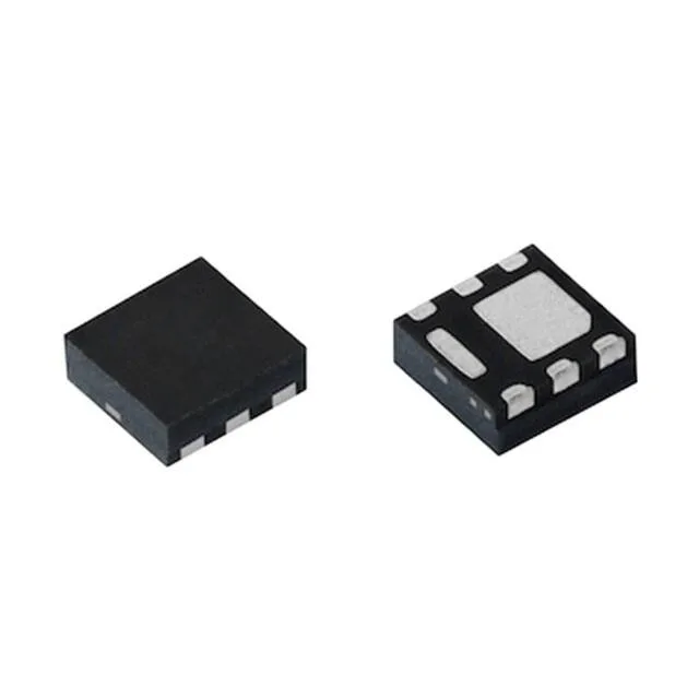
PowerPAK SC-70W-6 — wettable flank for AOI
The 6-PowerVDFN package with wettable flank terminals means the side of each lead is plated for solder wetting — automated optical inspection (AOI) can verify the solder fillet on the side of the package, not just the bottom. This is a requirement for many automotive Tier-1s: without wettable flank, a bottom-only solder joint is invisible to AOI and the assembly is classed as a latent defect risk. A 2-layer board with a 1 oz copper pour under the pad drops the junction-to-ambient thermal resistance to about 40 °C/W; a 4-layer board with thermal vias cuts it to 25 °C/W.