Gate charge and switching speed
The SIHB120N60E-T5-GE3: These numbers tell the gate-drive designer how much current the driver must supply to hit the target switching frequency — a 45 nC gate charge at 100 kHz switching draws 4.5 mA average from the driver, well within the capability of a standard MOSFET driver IC. The 1562 pF input capacitance also influences the turn-on delay; a driver with 2 A peak source current charges the gate in roughly 23 ns, keeping switching losses manageable in hard-switched topologies.
Thermal and package integration
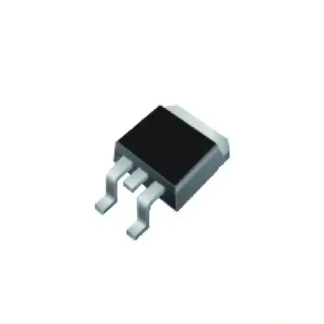
Housed in the D²PAK (TO-263) surface-mount package, the SIHB120N60E-T5-GE3 dissipates up to 179 W at the case. The exposed drain tab on the top of the package must be soldered to a copper pad on the PCB with adequate thermal vias to the inner ground plane — the junction-to-case thermal path is the limiting factor, not the package itself.