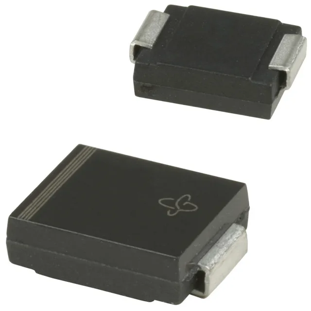
The 1.5SMC33CA-E3/9AT: At the full 32.8A peak pulse current, the voltage clamps at 45.7V maximum, so downstream silicon rated for 50V or higher sees a safe clamped waveform.
Clamping voltage and transient protection margin
The 45.7V maximum clamping voltage at Ipp sets the upper bound of the protected waveform. For a 24V rail with 20% tolerance (28.8V max), the 28.2V standoff provides 2.4V of headroom before the diode begins to avalanche. The bidirectional channel means the same device clamps both positive and negative transients symmetrically — useful on AC signal lines or DC rails subject to reverse polarity events. At 150°C junction, the peak pulse power derates linearly — the 1500W rating holds at 25°C, but at 125°C ambient the derating factor typically reduces available power to about 60% of the 25°C figure. For a design that must survive a 10/1000µs surge at 85°C ambient, the derated capability still exceeds 900W, leaving margin for most secondary lightning and inductive-load transients.
Package and board-fit for the DO-214AB footprint
The supplier device package is designated DO-214AB (SMCJ), and the tape-and-reel format (/9AT suffix) indicates 850 units per 13-inch reel. The copper pad area under the package body should match the recommended land pattern in Vishay's application note — a 4.5 mm × 4.0 mm pad per terminal with a 2.0 mm gap between them keeps the thermal impedance low enough to handle repetitive pulse trains without exceeding the 150°C junction limit.