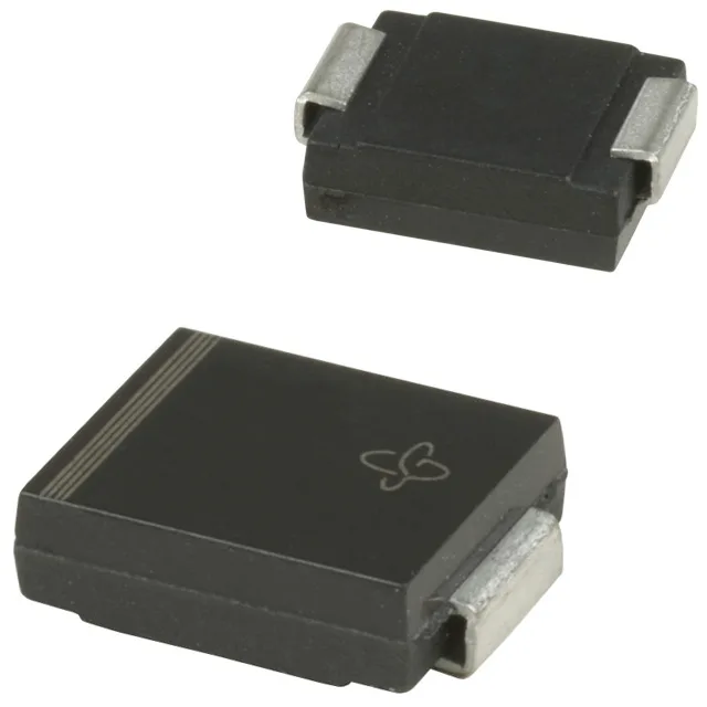
TVS diode selection for 12.8V rails
The 1.5SMC15AHM3_A/I: It clamps a 12.8 V reverse standoff rail at 21.2 V maximum, passing 70.8 A peak pulse current before the junction absorbs the transient. The 12.8 V standoff voltage suits 12 V nominal automotive power buses where the steady-state rail stays below the breakdown knee at 14.3 V minimum.
Clamping voltage and pulse current
The 21.2 V maximum clamping voltage at 70.8 A peak pulse current defines the voltage stress the downstream ICs must survive. A 12 V ECU input stage with a 25 V abs-max rating has 3.8 V of headroom above the clamp — marginal for repetitive surges, so verify the transient immunity of the protected device against the full 21.2 V level. The 1500 W peak pulse rating is specified for the 10/1000 µs double-exponential waveform. For shorter pulses (8/20 µs, common in ESD testing), the peak power capability is higher — the 1.5SMC series derating curve in the Vishay application note scales the rating upward as pulse width decreases.
Package and board-fit
DO-214AB (SMC) surface-mount package with a 0.203-inch body width and gull-wing leads. The cathode band and laser marking identify the unidirectional orientation — the anode is the die attach pad on the bottom, so the PCB thermal pad under the package is the cathode node and carries the full pulse current to the ground plane. The 1500 W pulse dissipates through the junction-to-ambient thermal path. A 1-oz copper pad of at least 300 mm² on the cathode side keeps the junction temperature rise below the 150°C absolute maximum during a single 10/1000 µs pulse at 25°C ambient.
The DO-214AB package is a standard Vishay footprint shared across the 1.5SMC series, so second-source equivalents from other manufacturers are parametric matches but not pin-compatible without layout review — the pad geometry is the same, but the marking code and polarity orientation differ.