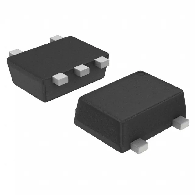
Toshiba Semiconductor RN1710JE(TE85L,F) — Memory (DRAM / SRAM / Flash / EEPROM)

RN1710JE(TE85L,F) Dual NPN Pre-Biased Transistor, 50V, 100mA

MPNRN1710JE(TE85L,F)
End of Life

Toshiba RN1710JE(TE85L,F) dual NPN pre-biased transistor, 50V VCEO, 100mA Ic, 250MHz fT, SOT-553 surface mount package, Tape & Reel.

$0.41Ref. price · indicative, final on quote
PackagingSOT-553
Sourced new & surplus through independent channelsAuthenticity-screened · ESD-safe packingListing updated Aug 2026

Specifications

RN1710JE(TE85L,F) specifications
ParameterValue
MountingSurface Mount
FET type2 NPN - Pre-Biased (Dual) (Emitter Coupled)
Voltage - collector emitter breakdown50V
Current - collector (Ic)100mA
Current - collector cutoff100nA (ICBO)
DC current gain (hFE) (Min) @ ic, vce120 @ 1mA, 5V
Power - max100mW
Frequency250MHz
PackageTape & Reel (TR); Cut Tape (CT)
CaseSOT-553
Resistor - base (R1)4.7kOhms
Vce saturation (Max) @ ib, ic300mV @ 250µA, 5mA

Product details

Dual pre-biased NPN in SOT-553

The Toshiba RN1710JE(TE85L,F) integrates two NPN transistors with internal bias resistors in a single SOT-553 package, each with a base resistor of 4.7 kΩ. The emitter-coupled pair shares a common emitter node, simplifying layout for differential or cascode stages where two matched transistors are needed.

250 MHz transition frequency

With a transition frequency of 250 MHz, this part can handle fast switching in signal conditioning, level translation, or oscillator circuits. The integrated bias resistors eliminate two external resistors per transistor, cutting BOM count and board area.

Frequently asked questions

What is the hFE of RN1710JE at 1 mA?

The DC current gain (hFE) is 120 minimum at 1 mA collector current with 5 V VCE.