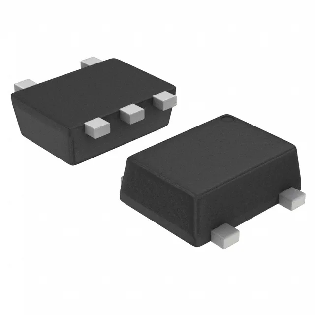
Toshiba Semiconductor RN1709JE(TE85L,F) — Memory (DRAM / SRAM / Flash / EEPROM)

Toshiba RN1709JE(TE85L,F) dual NPN pre-biased transistor

MPNRN1709JE(TE85L,F)
End of Life

Toshiba RN1709JE(TE85L,F) dual NPN pre-biased (BRT) transistor, 2 emitter-coupled NPNs with integrated R1=47kΩ, R2=22kΩ, 50V Vce, 100mA Ic, 250MHz ft, SOT-553 package, surface mount.

$0.41Ref. price · indicative, final on quote
PackagingSOT-553
Sourced new & surplus through independent channelsAuthenticity-screened · ESD-safe packingListing updated Aug 2026

Specifications

RN1709JE(TE85L,F) specifications
ParameterValue
MountingSurface Mount
FET type2 NPN - Pre-Biased (Dual) (Emitter Coupled)
Voltage - collector emitter breakdown50V
Current - collector (Ic)100mA
Current - collector cutoff500nA
DC current gain (hFE) (Min) @ ic, vce70 @ 10mA, 5V
Power - max100mW
Frequency250MHz
PackageTape & Reel (TR); Cut Tape (CT)
CaseSOT-553
Resistor - base (R1)47kOhms
Resistor - emitter base (R2)22kOhms
Vce saturation (Max) @ ib, ic300mV @ 250µA, 5mA

Product details

What this dual BRT saves you on the board

The Toshiba RN1709JE(TE85L,F) packs two NPN transistors with their bias resistors already on-die — a 47 kΩ base resistor (R1) and a 22 kΩ emitter-base resistor (R2) per side — into a single SOT-553 package. That means one component replaces two discrete transistors plus four resistors, which shrinks the pick-and-place count and frees up board area in a tight layout. The emitter-coupled pair configuration is handy for differential line receivers, current mirrors, or any low-side switch pair where you want matched Vbe tracking.

50 V, 100 mA — sizing the load

With a 50 V collector-emitter breakdown and 100 mA continuous collector current, this part fits 12 V, 24 V, and even 48 V industrial logic rails as long as the load stays under 100 mA. The 250 MHz transition frequency means it switches fast enough for PWM drive up to a few megahertz — plenty for relay coils, LED strings, or signal-level gate drive.

SOT-553 — tiny footprint, careful assembly

The SOT-553 package is about 1.6 mm × 1.6 mm, which is small enough to fit under a BGA shadow or on a cramped sensor module. The trade-off is that hand-soldering is impractical — you want a reflow profile matched to the package. The ESV supplier device package code tells you the die attach and wire bond variant Toshiba uses internally; for footprint purposes, stick to the SOT-553 land pattern in the datasheet.

Frequently asked questions

What is the difference between RN1709JE and RN1709?

The RN1709JE is the SOT-553 package variant; the base RN1709 typically comes in a larger package such as SOT-23 or SOT-323. The die and bias resistor values (47 kΩ / 22 kΩ) are the same, so the electrical performance is identical — the choice is purely a footprint and board-space decision.