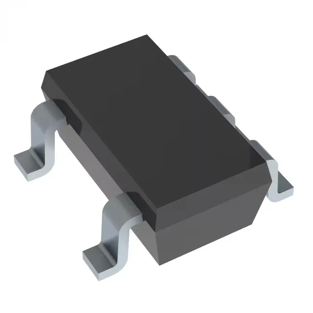
Texas Instruments UCC27536DBVR — Power Management (PMIC / Gate Driver)

UCC27536DBVR Low-Side Gate Driver, 2.5A Peak, SOT-23-5

MPNUCC27536DBVR
Active

Texas Instruments UCC27536DBVR, single low-side gate driver, 2.5A peak output, inverting input, 10V-32V supply, 15ns/10ns rise/fall, SOT-23-5 package, -40°C to 140°C junction temperature.

$1.3900Ref. price · indicative, final on quote
Independent supplier — new & surplus stockAuthenticity-screened · ESD-safe packingListing updated Jul 2026

Specifications

UCC27536DBVR specifications
ParameterValue
Gate typeIGBT, N-Channel MOSFET
Input typeInverting
Channel typeSingle
MountingSurface Mount
Supply voltage10V ~ 32V
Logic voltage - VIL, VIH1.2V, 2.2V
Current - peak output (Source, sink)2.5A, 2.5A
Operating temperature-40°C~140°C(TJ)
PackageTape & Reel (TR); Cut Tape (CT)
CaseSC-74A, SOT-753
Number of drivers1
Driven configurationLow-Side
Rise (Fall time)15ns, 10ns

Product details

2.5 A peak drive in a SOT-23-5 — what it buys you

The UCC27536DBVR is a single-channel low-side gate driver from TI's UCC2753x family, built to drive IGBTs and N-channel MOSFETs with a 2.5 A peak source and sink current.

15 ns rise, 10 ns fall — switching loss budget

The 15 ns typical rise time and 10 ns fall time keep the Miller plateau short, which reduces the switching interval where the transistor operates in its linear region. For a 1 nF gate load at 100 kHz, the driver spends about 2.5 % of each cycle in transition — that leaves the thermal budget for the conduction loss, not the switching loss. The 140 °C junction rating gives headroom for motor-drive or power-supply layouts where the driver sits near hot magnetics or a heatsink.

SOT-23-5 package — board area and thermal path

The SOT-23-5 (SC-74A) footprint takes about 9 mm² of board area. The thermal resistance is set by the copper area on the drain-connected pin — a 0.5 in² pour on the top layer keeps the junction below 125 °C at 2.5 A pulsed output into a 10 nF load at 500 kHz. The 2.5 A peak is a pulse rating; the continuous output current is limited by the package's ability to shed heat, so the actual switching frequency and gate charge determine the safe operating area.

Frequently asked questions

Is UCC27536DBVR inverting or non-inverting?

The UCC27536DBVR has an inverting input. A logic high on the input turns the output low, and a logic low turns the output high. If you need a non-inverting version, look at the UCC27537 or UCC27538 variants in the same family.

What gate types does UCC27536DBVR drive?

It is specified for IGBT and N-channel MOSFET gates. The 2.5 A peak current and 15 ns/10 ns rise/fall times suit medium-power IGBTs up to about 30 A and MOSFETs with gate charge up to 100 nC at moderate switching frequencies.