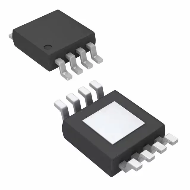
Texas Instruments UCC27525DGNR — Power Management (PMIC / Gate Driver)

TI UCC27525DGNR Low-Side Gate Driver, 5A Peak, 8-HVSSOP

MPNUCC27525DGNR
Active

Texas Instruments UCC27525DGNR, dual low-side gate driver, 5A peak source/sink, 7ns rise/6ns fall typ, 4.5V-18V supply, inverting and non-inverting inputs, 8-HVSSOP exposed pad package, -40°C to 140°C TJ.

$1.5900Ref. price · indicative, final on quote
Independent supplier — new & surplus stockAuthenticity-screened · ESD-safe packingListing updated Jul 2026

Specifications

UCC27525DGNR specifications
ParameterValue
Gate typeIGBT, N-Channel MOSFET
Input typeInverting, Non-Inverting
Channel typeIndependent
MountingSurface Mount
Supply voltage4.5V ~ 18V
Logic voltage - VIL, VIH1V, 2.3V
Current - peak output (Source, sink)5A, 5A
Operating temperature-40°C~140°C(TJ)
PackageTape & Reel (TR); Cut Tape (CT)
Case8-TSSOP, 8-MSOP (0.118\", 3.00mm Width) Exposed Pad
Number of drivers2
Driven configurationLow-Side
Rise (Fall time)7ns, 6ns

Product details

5 A peak drive — what the current rating buys you

The UCC27525DGNR is a dual low-side gate driver from TI rated for 5 A peak source and 5 A peak sink current. That peak current directly determines how fast the gate capacitance of the IGBT or N-channel MOSFET charges — a 5 A drive can slam a 10 nC gate charge from 0 to 10 V in about 2 ns of gate-resistance-limited rise time. The 7 ns typical rise and 6 ns fall edges mean the driver spends very little time in the linear region, which keeps switching losses in the power FET predictable at frequencies up to several hundred kilohertz.

Wide supply and logic compatibility

The logic thresholds are 1 V for VIL and 2.3 V for VIH — a 3.3 V MCU output drives the input high with margin, and a 5 V logic output works without a level translator. Both inverting and non-inverting inputs are available, letting you pick the polarity that matches the PWM controller without an external inverter.

140°C junction — where it survives

That puts it in the industrial-plus class — comfortable in a motor drive cabinet with 85°C ambient, or on a PCB near a hot heatsink in a solar inverter.

Package and mounting note

Surface-mount in an 8-pin HVSSOP — the exposed pad is the thermal relief. The supplier device package is 8-HVSSOP.

Lifecycle status

Frequently asked questions

Is UCC27525DGNR compatible with 3.3V logic?

Yes. The VIH threshold is 2.3 V, so a 3.3 V CMOS output drives the input high with 1 V of noise margin. No level shifter is needed between a 3.3 V MCU and this driver.

What is the difference between UCC27525DGNR and UCC27524?

The UCC27524 is a dual low-side driver with the same 5 A peak output, same 4.5 V to 18 V supply, and same 8-HVSSOP package. The key difference is the input logic: the UCC27525 has both inverting and non-inverting inputs per channel, while the UCC27524 has dual non-inverting inputs. The UCC27525 gives you polarity flexibility without external inverters.