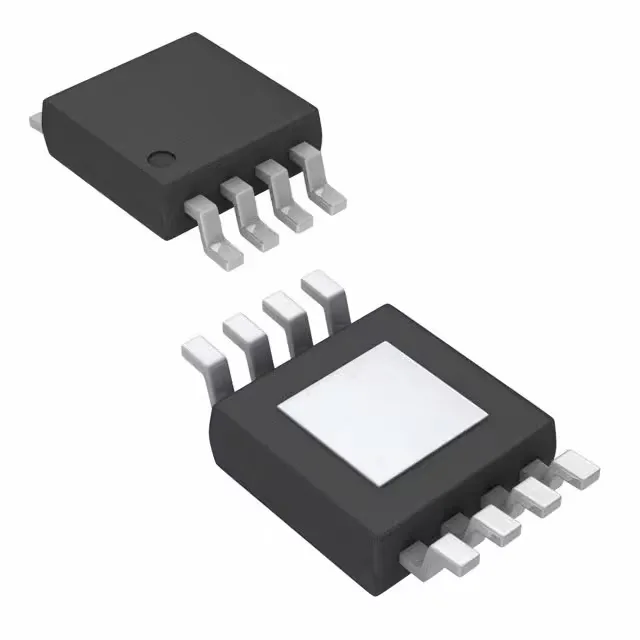
Texas Instruments UCC27425DGNR — Power Management (PMIC / Gate Driver)

UCC27425DGNR Gate Driver, 4A Peak, Dual N/P-Channel

MPNUCC27425DGNR
Active

Texas Instruments UCC27425DGNR, dual low-side gate driver, 4A peak source/sink, N-Channel and P-Channel MOSFET drive, 4V to 15V supply, 8-HVSSOP package, -40°C to 125°C.

$0.6600Ref. price · indicative, final on quote
Independent supplier — new & surplus stockAuthenticity-screened · ESD-safe packingListing updated Jul 2026

Specifications

UCC27425DGNR specifications
ParameterValue
Gate typeN-Channel, P-Channel MOSFET
Input typeInverting, Non-Inverting
Channel typeIndependent
MountingSurface Mount
Supply voltage4V ~ 15V
Logic voltage - VIL, VIH1V, 2V
Current - peak output (Source, sink)4A, 4A
Operating temperature-40°C~125°C(TA)
PackageTape & Reel (TR)
Case8-TSSOP, 8-MSOP (0.118\", 3.00mm Width) Exposed Pad
Number of drivers2
Driven configurationLow-Side
Rise (Fall time)20ns, 15ns

Product details

Dual 4A low-side driver for mixed-polarity gates

It is designed to drive both N-channel and P-channel MOSFETs from independent, inverting or non-inverting inputs, making it a single-component solution for power stages that mix polarity — synchronous buck converters, half-bridge topologies, and push-pull stages where the high-side is P-channel and the low-side is N-channel.

20 ns edges at 4 A — layout discipline required

The 20 ns typical rise time and 15 ns typical fall time at 4 A peak output mean the driver can charge and discharge a MOSFET gate capacitance quickly enough to keep switching losses low in the 100 kHz to 500 kHz range. Those edge rates also mean the loop from driver output through the gate resistor and back through the source return must be kept under 1 cm to avoid gate-voltage ringing that exceeds the MOSFET's Vgs rating.

The supply range from 4 V to 15 V lets this driver run directly from a 5 V logic rail or a 12 V bias supply without an intermediate regulator. The independent channel architecture means one channel can switch an N-channel MOSFET while the other drives a P-channel device on a separate timing domain.

The base product number UCC27425 covers a family of pin-compatible options (single vs dual, different output current grades), so if a future design needs a higher drive current the PCB footprint stays the same. The 8-HVSSOP package with exposed pad is a standard TI leadframe — no exotic substrate that might get cut early.

Sourcing: quoted to order per BOM quantity

No minimum order quantity is assumed; single-reel and partial-reel quantities are quoted on request.

Frequently asked questions

Can UCC27425DGNR drive both N-channel and P-channel MOSFETs?

Yes. The gate type is specified for both N-Channel and P-Channel MOSFETs. Each of the two independent channels can drive either polarity, with inverting or non-inverting input logic per channel.

What is the typical output current of UCC27425DGNR?

The peak output current is 4 A for both source and sink per channel. This is the peak rating at the output pin; the average current depends on switching frequency, gate charge, and duty cycle.

Is UCC27425DGNR RoHS compliant and lead-free?

The DGNR suffix indicates a lead-free, RoHS-compliant finish on the 8-HVSSOP package. The part is suitable for assembly in RoHS-compliant production lines without exemption paperwork.

What is the difference between UCC27425DGNR and UCC27424?

The UCC27425 and UCC27424 are pin-compatible dual low-side drivers in the same family. The primary difference is the logic input configuration: the UCC27425 offers independent inverting and non-inverting inputs per channel, while the UCC27424 has dual non-inverting inputs. Both deliver 4A peak output and share the same supply range and package options.