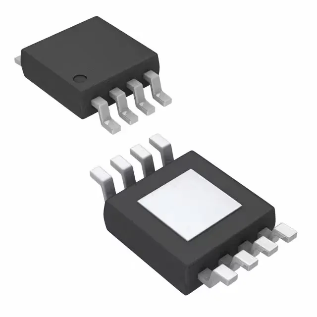
Texas Instruments UCC27325DGNR — Power Management (PMIC / Gate Driver)

TI UCC27325DGNR Dual Low-Side Gate Driver, 4A Peak, 8-HVSSOP

MPNUCC27325DGNR
Active

Texas Instruments UCC27325DGNR, dual low-side gate driver, N-Channel/P-Channel MOSFET, 4A peak source/sink, 20ns rise/15ns fall, 4.5V-15V supply, -55°C to 150°C, 8-HVSSOP exposed pad, Tape & Reel.

$0.6000Ref. price · indicative, final on quote
Independent supplier — new & surplus stockAuthenticity-screened · ESD-safe packingListing updated Jul 2026

Specifications

UCC27325DGNR specifications
ParameterValue
Gate typeN-Channel, P-Channel MOSFET
Input typeInverting, Non-Inverting
Channel typeIndependent
MountingSurface Mount
Supply voltage4.5V ~ 15V
Logic voltage - VIL, VIH1V, 2V
Current - peak output (Source, sink)4A, 4A
Operating temperature-55°C~150°C(TJ)
PackageTape & Reel (TR)
Case8-TSSOP, 8-MSOP (0.118\", 3.00mm Width) Exposed Pad
Number of drivers2
Driven configurationLow-Side
Rise (Fall time)20ns, 15ns

Product details

4A peak drive — what it buys the switching stage

The UCC27325DGNR is a dual low-side gate driver from Texas Instruments, rated for 4A peak source and 4A peak sink current. That 4A capability means it can slam the gate of a large MOSFET or IGBT on and off fast, keeping switching losses low even at high PWM frequencies. The 20 ns rise and 15 ns fall times (typical) confirm the edge speed — you get clean transitions without the Miller plateau hang that slower drivers leave.

Supply rail and logic interface

The supply range runs from 4.5 V to 15 V, so it works off a 5 V logic rail or a 12 V gate-drive rail without a separate regulator. The logic thresholds are 1 V for VIL and 2 V for VIH, which means 3.3 V logic from an MCU or FPGA drives it directly — no level shifter needed between the controller and the gate.

Two independent channels, any polarity

Each of the two drivers operates independently, and each input accepts both inverting and non-inverting signals. That lets you drive an N-channel low-side FET with one channel and a P-channel high-side FET with the other, or run both channels in parallel for a single 8A peak drive into a bigger load. The driven configuration is low-side, so plan for the load between the drain and the positive rail.

It comes in an 8-HVSSOP package (3.00 mm wide, exposed pad). The 8-MSOP footprint is standard; the pad pitch is 0.65 mm, fine for hand rework with a hot-air station but tight for a soldering iron.

Frequently asked questions

Is UCC27325DGNR pin compatible with UCC27324?

The UCC27325 and UCC27324 share the same base function and package footprint, but the UCC27325 offers 4A peak drive versus the UCC27324's 4A as well — check the input logic polarity options on the datasheet to confirm pin-for-pin compatibility in your specific layout.

What are the specifications of UCC27325DGNR?

It is a dual low-side gate driver with 4A peak source/sink current, 20 ns rise and 15 ns fall times, supply range 4.5 V to 15 V, operating junction temperature -55°C to 150°C, and an 8-HVSSOP exposed-pad package. It drives both N-channel and P-channel MOSFETs with independent inverting or non-inverting inputs.