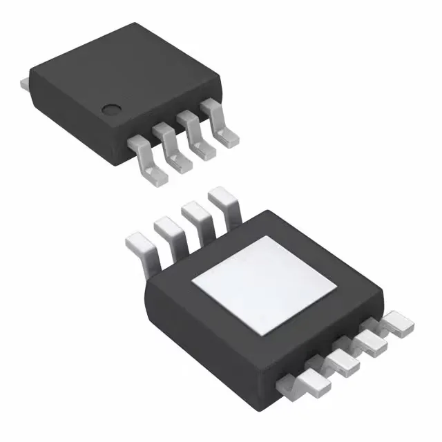
9 A peak output — what it buys the switching stage
The UCC27322DGNR is a single-channel low-side gate driver from Texas Instruments, rated for 9 A peak source and 9 A peak sink current. That peak current capability directly determines how fast the gate of a power MOSFET or IGBT charges and discharges — a 9 A driver can slam a 100 nC gate charge on or off in roughly 11 ns, which keeps switching losses low in a 200–500 kHz converter.
20 ns rise and fall — timing budget for the power loop
In practice, the actual edge rate depends on the total gate charge of the driven FET and the series gate resistor. The 20 ns figure tells you the internal output stage is fast enough that the external gate resistor — not the driver — will dominate the turn-on dV/dt, which is exactly what you want for controlling EMI and ringing in the power loop.
Logic thresholds are 1.1 V (VIL) and 2.7 V (VIH), so a 3.3 V PWM signal from an MCU or DSP will reliably drive the input — no level-shifter needed. The non-inverting input type means the output follows the input polarity, which simplifies the control loop.