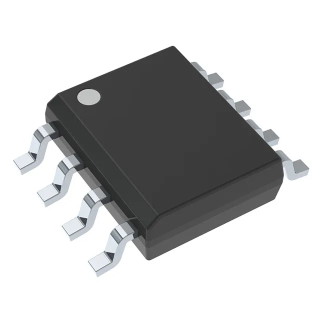
Half-bridge driver for automotive N-channel MOSFETs
The UCC27282QDQ1 is a Texas Instruments half-bridge gate driver designed for N-channel MOSFETs in automotive power stages. It drives two independent channels with non-inverting inputs, delivering 2.5A peak source and 3.5A peak sink current to charge and discharge the gate capacitance quickly. The bootstrap high-side supply is rated to 120 V maximum, making the part suitable for 48 V and 72 V automotive bus architectures as well as lower-voltage DC-DC converters.
The supply voltage range is 5.5 V to 16 V, covering standard automotive battery rails from a 12 V nominal system through load-dump transients. Logic input thresholds are 0.9 V (VIL) and 2.4 V (VIH), compatible with 3.3 V and 5 V microcontrollers without external level shifting. Rise and fall times are 12 ns and 10 ns typical — the faster fall edge helps minimise dead-time overlap when driving large MOSFETs in synchronous rectification stages.
Active production, 8-SOIC package
It is supplied in a tube and also available in tape-and-reel variants under the base product number UCC27282. No exposed thermal pad — junction-to-ambient thermal resistance is managed through copper pour area on the drain connections.