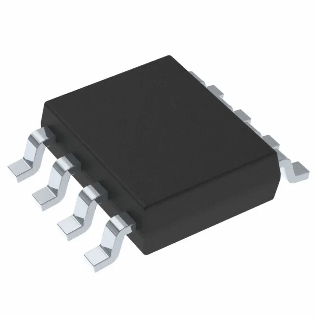
Half-bridge driver for 48V–72V automotive power stages
The Texas Instruments UCC27200QDDARQ1 is an automotive-grade half-bridge gate driver qualified to AEC-Q100, designed to drive two N-channel MOSFETs in an independent, non-inverting configuration. The bootstrap high-side voltage is rated to 120V maximum, which covers 48V and 72V automotive bus architectures as well as industrial power supplies up to 100V.
3A peak gate drive — sizing the switching loss budget
The 3A peak source and sink current is the headline rating that determines how quickly the driver can charge and discharge the MOSFET gate capacitance. With 8ns rise and 7ns fall times, the driver can switch a 10 nC gate load in under 15 ns, which keeps cross-conduction dead-time short and reduces switching losses in high-frequency converters. The buyer should verify that the total gate charge of the selected MOSFET does not exceed the driver's peak current capability at the intended switching frequency — a 60 nC gate at 500 kHz draws an average 30 mA from the driver, well within the 3A peak rating. The logic input thresholds are specified at 3V (VIL) and 8V (VIH), which are compatible with 3.3V and 5V PWM controllers from most MCUs and digital isolators. The 8V VIH minimum means a 5V logic signal will reliably trigger the high-side input, but a 3.3V signal may not reach the threshold — a level shifter or pull-up to the driver supply is needed for 3.3V logic.
Package and thermal management for the 8-SO PowerPad
Without the pad soldered, junction temperature rise will exceed the 140°C limit under continuous 3A peak drive at high duty cycles. The 8-SO PowerPad footprint is identical to a standard SOIC-8 with an additional centre pad; existing layouts for the UCC27200 base part number are directly compatible.
This eliminates the supply-chain risk of an imminent obsolescence-driven redesign for automotive or industrial programs with multi-year production runs. The base product number UCC27200 shares the same die and package; the Q1 suffix denotes the automotive AEC-Q100 qualification and the extended temperature range.