What this level shifter does on your board
The output type is tri-state, non-inverted, and the single-circuit device supports four channels per package.
The 100 Mbps data rate covers most SPI, UART, I2C (fast-mode plus), and general-purpose GPIO level-shifting needs. If your design runs a high-speed parallel bus or a multi-megabit serial link above 100 Mbps, this part will not keep up — consider a faster translator like the TXU0304BQAR (200 Mbps) or SN74LXC2T45DTTR (420 Mbps) for those cases. The auto-direction sensing eliminates the direction pin that older level shifters (e.g., 74LVC4245) require, which saves a GPIO on the microcontroller and simplifies firmware — no toggling of a DIR line on every bus turn-around. However, the auto-sense circuit adds a propagation delay and output-enable settling time; for push-pull signals below 100 Mbps it works transparently, but open-drain buses (I2C) may need an external pull-up and careful timing analysis.
Supply rails and voltage compatibility
This covers the common low-voltage cores (1.2 V, 1.8 V, 2.5 V, 3.3 V) on the A side and the higher-voltage peripherals (3.3 V, 5 V) on the B side. The 1.2 V minimum on VCCA means it can interface directly with the newest 1.2 V FPGAs and MCUs. Note that VCCA must always be less than or equal to VCCB — the part does not support stepping down from a higher A-side voltage to a lower B-side voltage. The supply sequencing is not critical as long as both rails are within the specified range, but TI recommends powering VCCA first or simultaneously to avoid undefined output states during ramp-up.
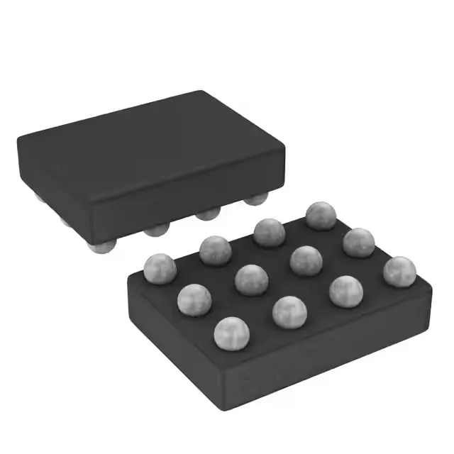
The 12-DSBGA package measures 1.9x1.4 mm with a 0.5 mm ball pitch. This is a wafer-level chip-scale package (DSBGA) — no leads, just solder balls on the bottom. The supplier device package code is 12-DSBGA (1.9x1.4).
It is ROHS3 compliant.