PSRR bandwidth and supply rail noise rejection
The TPS72017YZUT delivers 85 dB of PSRR at 10 Hz, rolling off to 50 dB at 1 MHz. For a precision analog front-end powered from a switching regulator, that 85 dB at low frequencies knocks down the 100/120 Hz ripple from the upstream converter by a factor of roughly 18,000 — the output rail stays clean enough that a 16-bit ADC's reference input sees no measurable line-frequency spurs. Above 100 kHz the PSRR drops, so if the switcher runs at 500 kHz, the attenuation at that frequency is below 50 dB; a second-stage LC filter ahead of the LDO may be needed to keep the noise floor under the ADC's LSB.
Dropout voltage and headroom budget
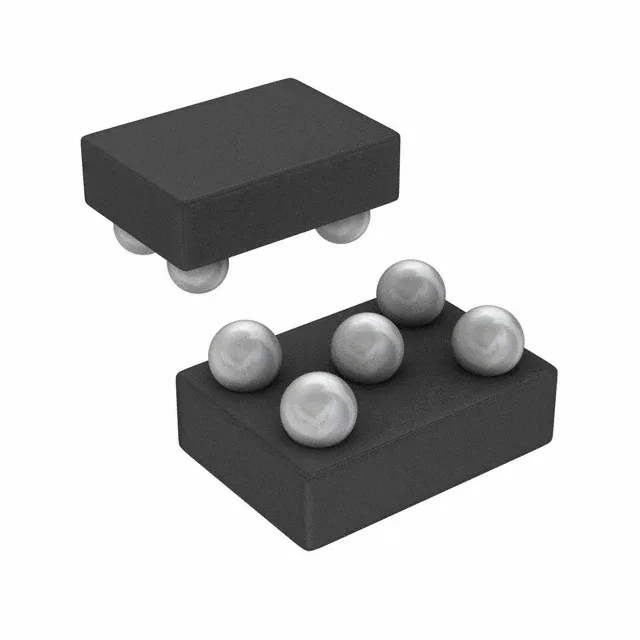
Maximum dropout is 0.2 V at the full 350 mA load. That means the input rail must stay at least 200 mV above the 1.7 V output across the full load and temperature range — a 1.9 V rail is the practical minimum. If the input is a 3.3 V bus, the 1.6 V headroom is fine, but the power dissipated in the pass element at 350 mA is 0.56 W; in the 5-DSBGA package with its 0.96x1.33 mm footprint, that heat must be sunk through the board copper. A 2-layer board with a thermal via under the package pad keeps the junction below the 125°C limit.
Quiescent current and always-on suitability
The 38 µA quiescent current (80 µA max supply current) makes this LDO a candidate for battery-powered always-on rails — a sensor node that sleeps most of the time and wakes to take a reading sees the LDO's own draw as a fixed overhead. At 38 µA, a 500 mAh coin cell would last over a year just powering the regulator before the battery self-discharge becomes the limiting factor.
Protection features for robust operation
Built-in overcurrent, overtemperature, and undervoltage lockout (UVLO) protect the load and the regulator. The UVLO threshold prevents the output from turning on until the input rail is high enough to keep the pass element in regulation — avoids the brown-out condition where the output tracks the input during a slow ramp. Overtemperature shutdown kicks in around 160°C junction, so a sustained short on the output folds back the current and lets the die cool before re-enabling.
That is a tiny BGA — the solder balls are under the die, not around the periphery, so visual inspection of the joints is impossible without X-ray. The reflow profile must follow TI's recommended peak temperature of 260°C for lead-free solder; the package is moisture-sensitive, so a bake at 125°C for 8 hours is required if the sealed bag humidity indicator card shows >10% RH. The supplier device package designation is 5-DSBGA (0.96x1.33) — this is the exact footprint for the PCB land pattern.