3.2 A buck plus 280 mA LDO — dual-rail automotive PMIC
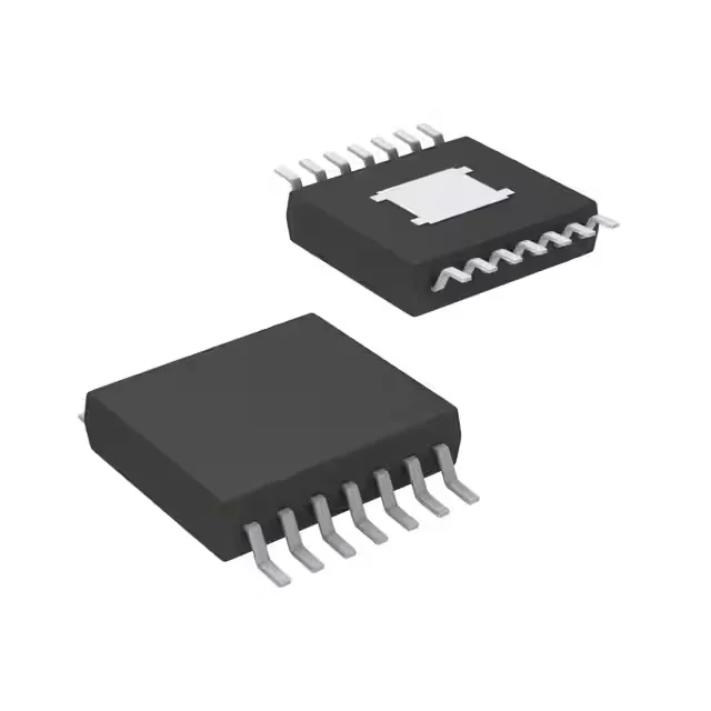
The TPS65320CQPWPRQ1 is a Texas Instruments automotive-grade power management IC combining a step-down (buck) converter rated for 3.2 A output with a 280 mA linear (LDO) regulator in a single 14-HTSSOP package. It accepts a supply from 3.6 V to 36 V, covering 12 V and 24 V automotive bus transients including cold-crank and load-dump events. The buck output is adjustable from 1.1 V to 20 V; the LDO provides a clean secondary rail from 1.1 V to 5.5 V. Switching frequency is programmable from 100 kHz to 2.5 MHz, allowing trade-offs between inductor size and efficiency.
AEC-Q100 Grade 1 — 125°C ambient capability
For a BOM targeting production vehicles or heavy equipment, this grade is the baseline — not a bonus.
NRND — last-time-buy planning required
Availability and date codes vary; confirm your quantity and required delivery window at quote time. No official pin-compatible successor is listed in the TI documentation, so any replacement will require a board respin.
14-HTSSOP thermal pad — layout consideration
The 14-HTSSOP package has an exposed thermal pad (PowerPAD) on the underside. The buck converter's 3.2 A output generates significant heat; the PCB copper area beneath the pad sets the junction-to-ambient thermal resistance. A four-layer board with thermal vias to an internal ground plane is standard practice for this part. The 0.65 mm pin pitch is manageable on two-layer boards for the control signals, but the power path demands wider traces.