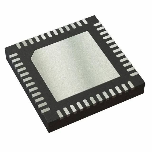
Seven-rail processor PMIC in a 6x6 QFN
The processor application target means the output sequencing and voltage accuracy are tuned to the power-up requirements of a typical SoC or MPU — the datasheet's sequencing timing should be checked against the processor's power-good window.
The 2.2 V minimum input lets the PMIC run from a deeply discharged Li-ion cell or a 2.5 V intermediate rail, while the 5.5 V ceiling covers 5 V USB and 5 V system supplies. The seven outputs are multiple — not all necessarily adjustable — so the BOM designer must confirm each rail's voltage and current capability against the processor's core, I/O, PLL, and memory-supply demands. Compare this with the single-output TPS53317RGBR (DDR converter, 1.0 V input, 85°C max) or the TPS51100DGQ (single DDR termination, 4.75 V input, 85°C max) — those are point-of-load regulators for one rail, not a multi-output PMIC. The TPS6521855RSLT replaces a cluster of separate converters with one sequenced controller, saving board area and simplifying the power-up handshake.
Confirm the exact voltage and current per output against the processor datasheet before locking the design — the PMIC's output configuration is fixed at the factory, not field-programmable.