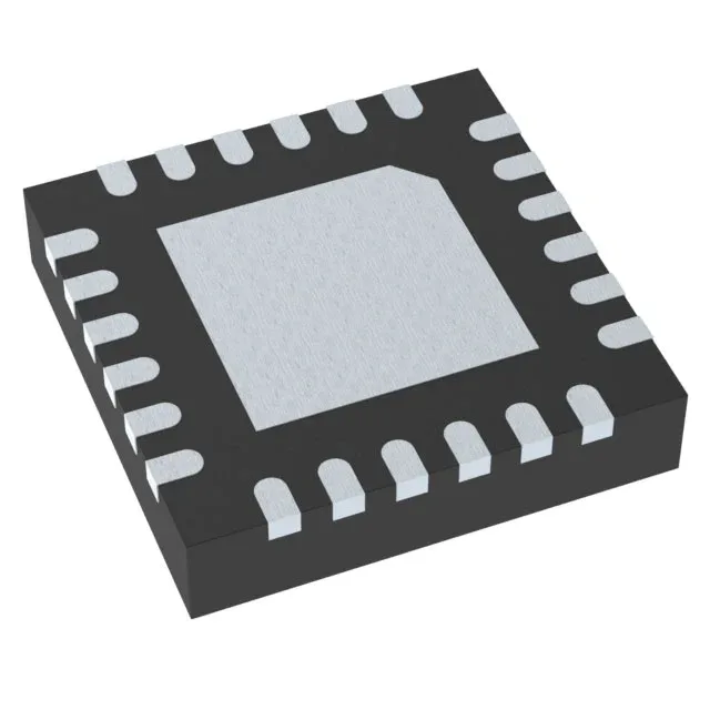
Texas Instruments TPS65110RGER — Power Management (PMIC / Gate Driver)

TI TPS65110RGER triple-output charge pump, -2.7V/3.3V/7.5V

MPNTPS65110RGER
Obsolete

Texas Instruments TPS65110RGER triple-output charge pump IC, LTPS LCD bias, -2.7V/3.3V/7.5V outputs, 2.4V-5.5V input, -40°C to 85°C, 24-VFQFN exposed pad.

$1.0700Ref. price · indicative, final on quote
Independent supplier — new & surplus stockAuthenticity-screened · ESD-safe packingListing updated Jul 2026

Specifications

TPS65110RGER specifications
ParameterValue
MountingSurface Mount
Voltage - input2.4V ~ 5.5V
Voltage - output-2.7V, 3.3V, 7.5V
I/O channels3
Operating temperature-40°C~85°C
PackageTape & Reel (TR); Cut Tape (CT)
ApplicationsCharge Pump, LTPS LCD
Case24-VFQFN Exposed Pad

Product details

Triple-rail bias for LTPS LCD — -2.7V, 3.3V, 7.5V

The Texas Instruments TPS65110RGER is a triple-output charge pump IC purpose-built for low-temperature poly-silicon (LTPS) LCD panel bias. It delivers three regulated rails: -2.7V, 3.3V, and 7.5V from a single 2.4V to 5.5V input supply — covering the gate-on, logic, and gate-off voltages that LTPS panels require. This is not a general-purpose PMIC.

New designs should not target this device; existing BOM lines must source through the surplus and broker channel. For sustainment programs already locked to this rail set, we source the TPS65110RGER to order against an RFQ.

Package and thermal — 24-VFQFN with exposed pad

Housed in a 24-VFQFN exposed-pad package (4x4 mm body, supplier device package 24-VQFN), the TPS65110RGER requires a thermal-land pattern on the PCB to sink heat from the charge pump switches.

Not qualified for under-hood or engine-bay environments.

Frequently asked questions

What is the replacement for TPS65110RGER?

No official replacement part number is recorded in the lifecycle documentation. The TPS65110RGER is obsolete with no direct pin-compatible successor from Texas Instruments. For new designs, evaluate a general-purpose triple-output PMIC or a dedicated LTPS bias IC from the TPS651xx family — but verify pinout and output voltage set against your BOM. For existing production, source the original TPS65110RGER through independent distribution against an RFQ.

What are the exact output voltages of TPS65110RGER?

The three regulated outputs are -2.7V, 3.3V, and 7.5V. These are fixed rails for LTPS LCD gate-on, logic, and gate-off bias respectively.

What package does TPS65110RGER use?

24-VFQFN exposed pad (4x4 mm body), also referred to as 24-VQFN.