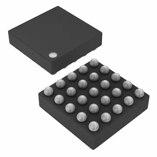
Four-rail PMIC in a 25-bump wafer-level package
The Texas Instruments TPS65030YZKR is a power-management IC packing three charge-pump converters and one linear LDO regulator into a 25-bump DSBGA package. It delivers four independent output rails from a 3 V to 5 V input bus — a topology choice that tells you this was designed for battery-powered portables where inductor-based switchers were too tall or too noisy for the nearby RF section. Output 1 provides 5 V at 100 mA — typically the USB or audio-codec rail. Output 2 delivers 1.5 V at 200 mA, likely the core supply for a low-voltage processor or memory. Output 3 is 3.3 V at 22 mA, sized for the I/O or always-on domain. The fourth output is the LDO, which cleans up whichever rail needed post-regulation.
Charge-pump topology — no inductors, no magnetic noise
All three switched-capacitor converters run at 1 MHz, which keeps the flying capacitors small enough for 0402 or 0603 ceramics. The trade-off is efficiency — charge pumps typically hit 85-90% at light load, versus 90-95% for an inductor-based buck. But in a Bluetooth headset or a portable medical monitor, the absence of inductor radiated noise can be the deciding factor for passing radiated emissions.
Industrial temperature range, but no supervisor or sequencer
Note that the part has no built-in power-on sequencer or supervisor, so the board designer must sequence the four rails externally or rely on the load devices' own POR thresholds.