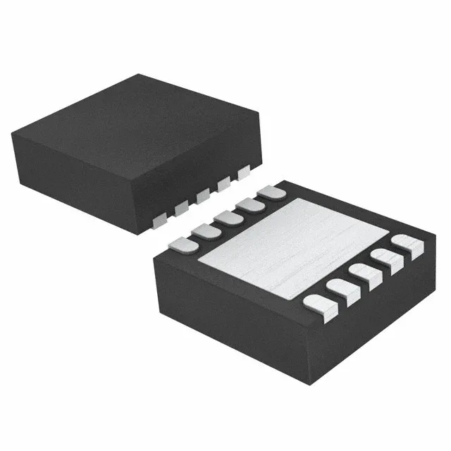
900 mA switch in a 2.5x2.5 mm footprint
Its 2.4 MHz switching frequency lets you use a small inductor and ceramic capacitors, keeping the total solution area tight — the 10-WFDFN package with exposed pad (2.5x2.5 mm) is the dominant footprint.
Efficiency stack-up over temperature
Synchronous rectification eliminates the external Schottky diode, cutting the forward-drop loss that eats into battery life at light loads. The 2.4 MHz switching frequency pushes ripple into the 2.4 MHz band, so the output capacitor ESR contribution to ripple is lower than a 500 kHz design — but the switching losses in the FETs rise with frequency, so the efficiency peak sits in the 100 mA to 500 mA load range typical of portable devices.
Package and thermal: the exposed pad is non-negotiable
The supplier device package is 10-SON (2.5x2.5 mm). Without a thermal-via array under the pad to conduct heat into the inner ground layers, the junction temperature rises above the 85°C ambient limit at full 900 mA switch current. The datasheet recommends at least four vias in the pad area — a standard 0.3 mm via with 0.5 mm pitch works. The small footprint means the input and output capacitors sit close to the IC, which keeps the switching loop inductance low.