Fixed 3.3 V rail from a single-cell Li-Ion — no divider resistors needed
That fixed output means no external feedback resistor divider, saving two components and one potential noise injection point on a dense board. The 3.5 A switch current limit is the real headroom number: in a buck-boost, the switch handles the full input current plus the boost ratio, so a 3.5 A switch typically supports a continuous output of 2 A to 2.5 A depending on Vin and the inductor ripple. The 2.5 MHz switching frequency keeps the inductor small — 1 µH to 2.2 µH range — and pushes the switching noise above the AM band, which helps in RF-sensitive portable gear.
2.5 MHz switching — inductor size and noise placement
At 2.5 MHz the fundamental ripple is at 2.5 MHz and its harmonics, well above the 1.6 MHz AM radio band and most audio amplifier bandwidths. That frequency also lets you use a 1.0 µH to 2.2 µH inductor with a saturation rating above the 3.5 A switch peak — a 2.2 µH, 4 A part in a 3×3 mm footprint is typical. No external compensation is needed — the TPS63025 family uses internal compensation, so the BOM stays tight.
20-DSBGA — what the 0.4 mm pitch means for assembly
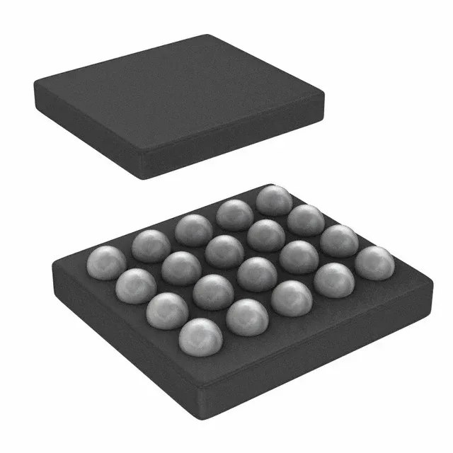
The 20-DSBGA is a 0.4 mm pitch wafer-level chip-scale package — 2.24 mm × 1.73 mm body, no mould compound. That demands a solder-mask-defined pad with a 0.225 mm NSMD opening and a 0.3 mm copper pad, plus a 0.1 mm solder-paste stencil aperture.
That means TI is still manufacturing this variant in the 20-DSBGA package, and the base product number TPS630252 is the design-in anchor — the YFFR suffix is the DSBGA reel variant. If you need a larger package for prototyping, the TPS630252 in a 12-pin QFN (RUK) is the same silicon in a 0.5 mm pitch, easier to hand-solder. No official second source is listed; this is a single-sourced TI part. For production, the BOM should carry a sole-source flag.