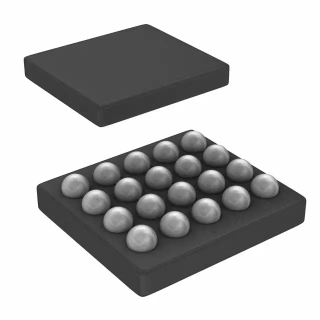
2.5 MHz buck-boost in a 20-bump DSBGA
The 2.5 MHz switching frequency lets the designer drop the inductor value to the 1 µH range and use small 0402/0603 ceramics, shrinking the total power-stage footprint — a clear fit for battery-powered portable devices, IoT endpoints, and space-constrained industrial sensors where board area is the binding constraint.
The 2.12 A switch current is the peak current the internal FET can carry cycle-by-cycle. In step-down mode (VIN > VOUT), the output current can approach the switch rating minus switching losses; in step-up mode (VIN < VOUT), the output current is lower by the boost ratio. For a 3.3 V output from a 2.5 V input, expect roughly 1.5 A continuous output — enough to power a small radio module, a sensor cluster, or an MCU with peripheral load.
20-DSBGA footprint and assembly
The 20-bump DSBGA uses a 0.4 mm ball pitch. The board requires a fine-line solder mask, a controlled stencil aperture (typically 0.22 mm square), and a reflow profile matched to the SAC305 alloy. This is not a hand-solder part — the assembly needs a pick-and-place line with vision alignment and a nitrogen-capable reflow oven for consistent wetting. The supplier device package is 20-DSBGA, identical to the case code. If the ambient in your enclosure exceeds 85°C, this part is not the fit.