Fixed 3.3 V rail from a 1.8–5.5 V input — no divider network
Because the output is fixed, no external resistor divider sets the voltage — the feedback network is internal, saving two components and one layout trace.
The 1.6 A switch current is the peak current the internal power FET can handle during each switching cycle. In a buck-boost topology, the output current is lower than the switch current — typically 800 mA to 1.2 A at 3.3 V, depending on input voltage and inductor ripple. If the BOM calls for 1.5 A continuous at 3.3 V, step up to the TPS63002 (2 A switch) or consider an external-FET design.
Switching at 1.25–1.5 MHz — inductor and noise trade-offs
The 1.25 MHz to 1.5 MHz switching frequency means the inductor value lands in the 2.2 µH to 4.7 µH range — a small, low-profile component that fits under a 3 mm height ceiling. The trade-off is switching loss: at 1.5 MHz the core and copper losses are higher than a 500 kHz part, but the smaller inductor saves board area. For noise-sensitive analog front-ends, the switching harmonics fall in the AM band, so a post-filter LC stage (10 µH + 10 µF) is recommended if the 3.3 V rail also powers an RF receiver.
Industrial temperature grade — deployment boundary
It is not AEC-Q100 qualified — if the target is under-hood automotive (125°C ambient), look at the TPS63001-Q1 variant which carries the automotive grade. For a 24/7 industrial controller running at 70°C internal ambient, the 85°C ceiling provides 15°C margin before thermal shutdown.
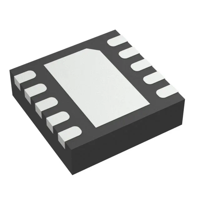
Package and footprint — 10-VSON with exposed pad
For a 1 A load, the pad temperature stays below 60°C with a 2-layer board and 1 oz copper, provided the via count is at least four.
No second-source cross-reference is listed on this record, but the TPS63001 base product number shares pin-compatibility across the family's output voltage options (1.8 V, 2.5 V, 3.3 V, adjustable).