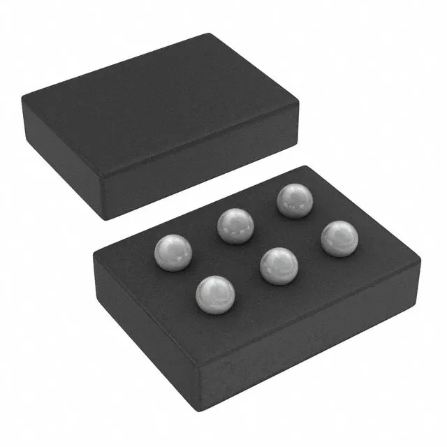
500 mA, 5.45 MHz synchronous buck in a 6-bump DSBGA
The TPS62674YFDR is a fixed-output step-down (buck) converter from Texas Instruments, delivering up to 500 mA from a 2.3 V to 4.8 V input rail. The output is fixed at 1.26 V, so no external feedback divider is needed — just the input and output caps and the inductor.
Package and temperature — what the DSBGA means for assembly
The part comes in a 6-bump DSBGA (6-XFBGA) package — 0.4 mm pitch, no leads, just solder balls on the bottom. This is a wafer-level chip-scale package; the die is essentially the package. That means the footprint is tiny, but the reflow profile needs to match the JEDEC standard for DSBGA, and the board must have a solder-mask-defined pad pattern. No underfill is required for most applications, but the small bump size means the PCB land should be non-solder-mask-defined (NSMD) for best reliability. The junction temperature limit is higher, but the 85°C ambient ceiling is the practical design-in number for the thermal budget.
For a production BOM, this part does not force a qualification requalification cycle in the near term.