6 MHz switching — why the small inductor matters
The 6 MHz switching rate lets you use a 0.47 µH to 1 µH inductor and 4.7 µF output capacitor — roughly half the footprint of a 1 MHz equivalent. That makes this part a fit for space-constrained portable or RF power rails where board area is the binding constraint, not raw efficiency.
1 A output at 1.2 V — load budget and thermal reality
With a fixed 1.2 V output and 1 A continuous rating, the TPS62665YFFT is sized for low-voltage core and I/O rails — think a 1.2 V DDR termination, an FPGA VCCINT rail, or a wireless SoC's digital supply.
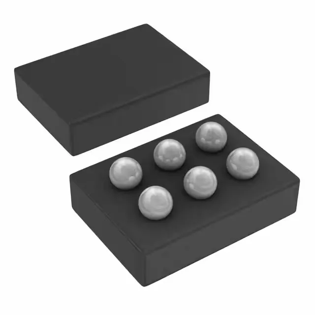
6-DSBGA — layout constraints for the board designer
Fan-out requires micro-vias (laser-drilled, 0.2 mm pad diameter) on a minimum 2-layer PCB; a 4-layer stack with a ground plane under the package improves thermal spreading. The input and output capacitors must sit within 2 mm of the package to keep the 6 MHz switching loop inductance below 2 nH.