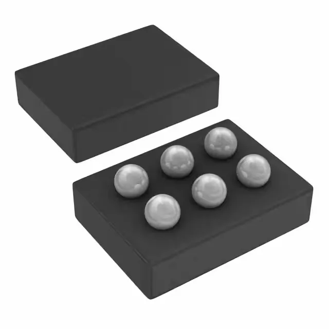
The 6-DSBGA package (six solder bumps, 0.4 mm pitch typical) is the smallest footprint you'll get for a 1 A regulator — roughly 1.5 mm × 1.5 mm — which means the inductor and output caps shrink accordingly. That 6 MHz switching rate lets you use a 0.47 µH or 1 µH inductor and 4.7 µF to 10 µF ceramic output caps, saving board area on a tight RF or sensor rail.
Hot-air profile for the DSBGA — will it survive rework?
The 6-DSBGA is a wafer-level chip-scale package — no mould compound, just the silicon die with solder bumps. That means the die is exposed on the top side; you need a gentle hot-air profile with a top preheat around 150°C to 160°C and a peak reflow at 245°C to 250°C (lead-free). The thermal mass is tiny, so it heats fast — keep the nozzle 2 mm to 3 mm above the part and watch for the bumps to collapse. Orientation is critical: the pin-1 indicator is a small dot on the top of the die, not a chamfered edge. If you lose the dot, you're guessing. A stencil with 0.3 mm to 0.35 mm apertures for the bumps and a 0.1 mm to 0.125 mm foil thickness works. No underfill is standard for this package, but if the board sees shock or vibration, a drop of low-viscosity underfill around the edge buys reliability.
Layout checklist — keeping the 6 MHz loop tight
At 6 MHz, the switching loop (input cap to VIN to SW to output cap back to GND) must fit under the part — the DSBGA bumps are the loop. Place the 10 µF input ceramic cap within 1 mm of the VIN and GND bumps, using 0.3 mm to 0.4 mm vias to the ground plane. The inductor (0.47 µH to 1 µH, low-DCR shielded type) sits next to the SW bump; keep the trace under 2 mm. Output cap goes between the VOUT bump and the load. The FB bump (if adjustable) is a high-impedance node — keep it clear of the SW and inductor field. A solid ground plane on layer 2 under the DSBGA helps thermal spreading, since the package has no exposed pad.