6 MHz buck — why the high frequency matters for your board
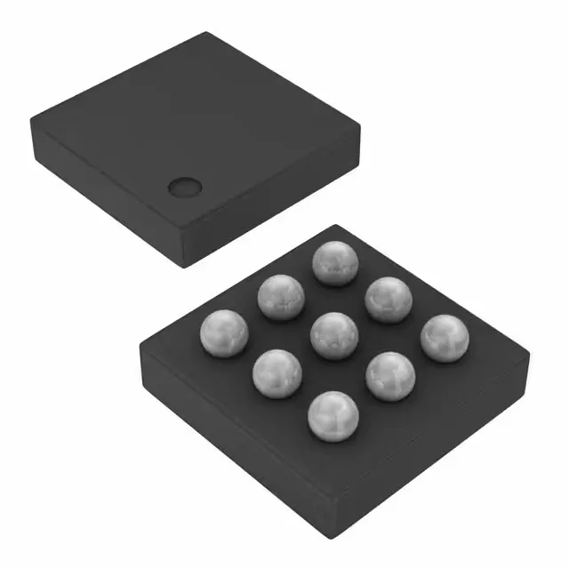
The TPS62650YFFR is a 6 MHz step-down (buck) converter from TI, built for applications where board area is the constraint, not switching losses. At 6 MHz, the inductor and output capacitors shrink to sub-millimeter footprints — think 0402 or 0603 passives — which is the whole point of picking this part over a 500 kHz or 1 MHz regulator. The 800 mA output current is enough for a sensor node radio, a small FPGA core rail, or a serial-interface supply, but the real win is the 9-bump DSBGA package that sits on a 1.6 mm² footprint.
Input range and output voltage — what fits
The output is adjustable (programmable) from a minimum of 0.75 V up to 1.44 V, with fixed 1.05 V and 1.2 V options available on the same die — the YFFR variant lets you set the voltage with external feedback resistors. That 0.75 V floor is useful for the latest low-voltage core rails on Cortex-M or FPGA fabrics.
9-DSBGA — what the package means for assembly and rework
The 9-DSBGA (die-size ball-grid array) is a 0.4 mm pitch, 9-ball package with no exposed thermal pad — all heat sinks through the solder balls into the board copper. On a field-service bench, swapping this part without a hot-air station is not realistic; the reflow profile is standard SAC305, but the 0.4 mm pitch demands a stencil aperture of 0.25 mm square and a placement machine with ±0.05 mm accuracy. No lab, no bench, let us go — but bring the hot air.
Synchronous rectification and efficiency
The TPS62650 integrates a synchronous rectifier, which means the low-side switch is a MOSFET instead of a Schottky diode. At 6 MHz, synchronous rectification recovers the body-diode conduction loss that would otherwise dominate the efficiency curve at light loads — expect >85 % efficiency down to 10 mA output in a well-laid-out board. The 800 mA continuous output is derated above 70°C ambient; at 85°C the part still delivers the full rated current if the board copper area is adequate.