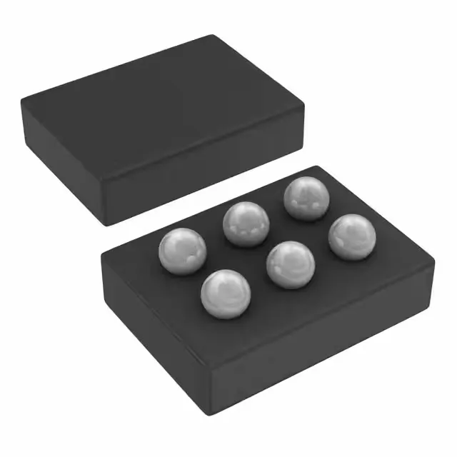
600 mA, 6 MHz buck in a 6-DSBGA — what the ratings mean
The TPS62624YFFT is a fixed 1.2 V output, 600 mA step-down converter switching at 6 MHz with an integrated synchronous rectifier. That switching frequency lets the output filter shrink to small ceramic capacitors and a tiny inductor, which is the whole point of the 6-DSBGA package — the total solution fits in a few square millimetres on the board. Input range is 2.3 V to 5.5 V, so it runs from a single lithium-ion cell (3.0–4.2 V) or a 5 V USB rail. The 1.2 V fixed output is common for core supplies on low-power MCUs and RF transceivers.
6-DSBGA footprint and what it asks of the layout
Package is 6-UFBGA, DSBGA — a 6-bump wafer-level chip-scale package with 0.50 mm pitch. The bottom-side bumps are the only electrical and thermal path; the PCB land pattern must match TI's recommended layout exactly, with via-in-pad under the bumps for thermal relief. No exposed paddle, no side-wettable flanks. Because the switching node is exposed on the bumps, the input capacitor (4.7 µF recommended) must sit as close as possible to the VIN and GND bumps to keep the switching loop small. A 6 MHz edge rate will radiate if the loop area is loose.