6 MHz switching — what it buys the board
Input range and output rail — BOM-fit check
The 2.3 V minimum input covers a deeply discharged single-cell Li-Ion battery; the 5.5 V maximum accepts a 5 V USB supply or a regulated 5 V rail with margin. The fixed 1.82 V output targets low-voltage core rails for DSPs, FPGAs, or DDR memory termination — no external resistor divider needed, which saves two components and one feedback-node noise path. The internal FETs handle the full 600 mA load with efficiency that peaks above 90 % at moderate loads, though the exact curve depends on the inductor and capacitor selection.
Package and assembly — DSBGA realities
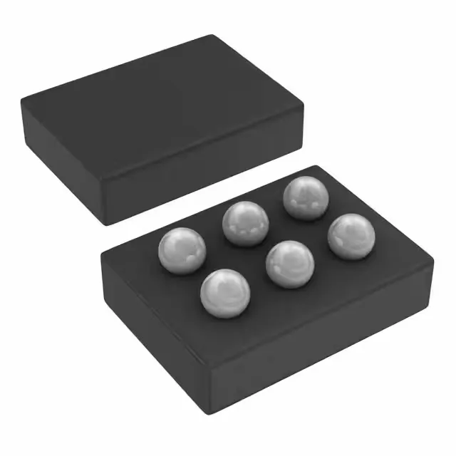
The 6-DSBGA package is a wafer-level chip-scale package. It requires a solder-mask-defined pad layout and a reflow profile matched to the JEDEC standard for lead-free assembly.
The 85°C ceiling is the ambient limit — junction temperature will be higher under full load, so a thermal analysis on the PCB copper area is needed for high-ambient or enclosed designs.