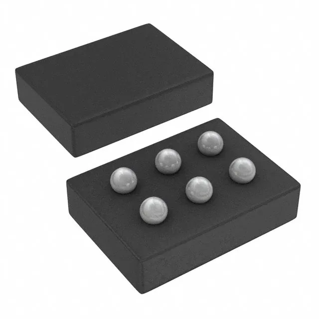
Texas Instruments TPS62612YFDT — Power Management (PMIC / Gate Driver)

TPS62612YFDT Texas Instruments Step-Down Buck, 6 MHz, 350 mA

MPNTPS62612YFDT
Active

Texas Instruments TPS62612YFDT step-down buck regulator, fixed 1.5 V output, 350 mA, 6 MHz switching, 2.3-5.5 V input, -40 to 85°C, 6-DSBGA package, synchronous rectifier.

$0.9103Ref. price · indicative, final on quote
Independent supplier — new & surplus stockAuthenticity-screened · ESD-safe packingListing updated Jul 2026

Specifications

TPS62612YFDT specifications
ParameterValue
Output typeFixed
MountingSurface Mount
Voltage - input5.5V
Voltage - output (Min (Fixed))1.5V
Output current350mA
Frequency - switching6MHz
I/O channels1
Operating temperature-40°C~85°C(TA)
PackageTape & Reel (TR); Cut Tape (CT)
FunctionStep-Down
TopologyBuck
Case6-XFBGA, DSBGA
Output configurationPositive
Synchronous rectifierYes

Product details

The TPS62612YFDT is a Texas Instruments step-down (buck) regulator switching at 6 MHz — that clock rate lets you use a 1 µH or smaller inductor and a 4.7 µF output capacitor, shrinking the total power-stage footprint to a few mm². For a board where every mm² is budgeted (wearable, IoT sensor, portable medical), this part saves real estate over a 1-2 MHz regulator that needs a 4.7 µH inductor and 10 µF cap.

Fixed 1.5 V rail — core supply for low-voltage logic

Output is fixed at 1.5 V — no external resistor divider needed. That voltage is a common core supply for FPGAs, MCUs, and wireless SoCs (e.g., CC13xx, certain STM32L4 parts). If your BOM calls for an adjustable output, this fixed version won't fit; look at the TPS62612 adjustable variant instead.

Input range and current — battery to regulated bus

The 350 mA output is sized for a small FPGA core (e.g., iCE40UP5K) or a wireless module drawing 200-300 mA peak. At 350 mA continuous, the 6-DSBGA package's thermal impedance (approx 150 °C/W) keeps junction temperature under 100 °C at 85 °C ambient — no derating needed for most designs.

6-DSBGA — footprint and layout

The 6-DSBGA (0.9 mm × 1.3 mm typical, 0.4 mm pitch) is a wafer-level chip-scale package. No exposed pad — all six balls carry the thermal path through the PCB vias. A 4-layer board with thermal vias under the package is recommended; a 2-layer board can work if the output current stays below 200 mA and the ambient is under 60 °C. The solder paste stencil aperture should match the ball diameter (0.25 mm typical) to avoid bridging.

Frequently asked questions

What is the output voltage of TPS62612YFDT?

Design engineers need the exact output voltage to validate circuit compatibility.

What is the price of TPS62612YFDT?

Buyers compare costs for BOM planning and budget approval.

Is TPS62612YFDT in stock?

Immediate availability drives purchasing decisions and lead time assessment.

What is the package of TPS62612YFDT?

Mechanical fit verification is critical for PCB layout and assembly.

What are the alternatives to TPS62612YFDT?

Designers and buyers need replacement options for sourcing flexibility or second sourcing.

Is TPS62612YFDT obsolete?

Lifecycle status determines long-term availability and risk of redesign.