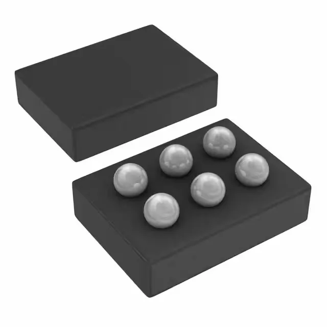
500 mA buck in a 1.5 mm² footprint
Switching at 6 MHz — what it buys you
At 6 MHz the output inductor can be in the 0.47 µH to 1 µH range, and the output capacitor around 4.7 µF. That shrinks the total solution footprint to fit under a 6-DSBGA package that measures roughly 1.5 mm × 1.5 mm. The trade-off is higher switching losses than a 1 MHz part, but at 500 mA the efficiency curve still peaks above 85 % for most of the load range. The synchronous rectifier (internal FET for the low-side switch) eliminates the external Schottky diode and keeps the efficiency up at light loads. That matters when the load drops to a few milliamps in sleep mode — the part doesn't waste power on a diode drop.
Package and temperature — what to plan for
The 6-DSBGA (0.5 mm pitch, 6-bump wafer-level chip-scale package) requires a controlled solder-paste stencil and a reflow profile matched to the board thickness. Store the reels dry — the DSBGA is moisture-sensitive, and a bake cycle before rework adds schedule time.